


Hardware components | ||||||
 |
| × | 1 | |||
| × | 1 | ||||
Software apps and online services | ||||||
| ||||||
As I explained in detail here, a robot is filled with embedded software and modules that have to work together to actualize the design goals. Image processing is one of the most challenging ones in this list of modules. It is very computationally expensive and it has to yield results in real-time.
In this blog, we are going to build a demo project to demonstrate the flexibility of Zynq UltraScale SOCs for implementing embedded vision applications. To do this, we use an Ultra96 board and connect to an MT9V034 global shutter image sensor. Then, we put an HLS based edge detector IP in the pipeline as the example accelerator. The hardware project will be used as an overlay for the Python Pynq where we configure the IPs and get the results.
HardwareThe basic architecture is illustrated in the following picture.
The MT9V034 camera sends out the pixels on its parallel 10bits data bus one by one and synchronous to a pixel clock signal. The beginning of each frame is indicated by the rising edge of a frame valid signal and the start of each line is marked by the line valid.
At the first step, The video to AXI stream block converts the parallel Bayer vide to a 16 bits standard AXI Video Stream. Then, the color interpolation IP converts this Bayer video to standard 24 bits RGB AXI stream. This is the standard video interface we work with for implementing the rest of the processing IPs.
In this project, we are going to detect the edges in the image coming from the camera. Thus, we implement the HLS Edge Detector IP using the HLS video library. The source code for this IP is simple and is as follows:
#include <ap_int.h>
#include <hls_video.h>
#include "ap_axi_sdata.h"
#define IMAGE_HEIGHT 480
#define IMAGE_WIDTH  752
using namespace hls;
typedef stream<ap_axiu<24,1,1,1> > AXI_STREAM;
typedef stream<ap_axiu<8,1,1,1> > AXI_STREAM_Mono;
typedef stream<ap_axiu<32,1,1,1> > AXI_STREAM_Result;
typedef hls::Mat<IMAGE_HEIGHT, IMAGE_WIDTH, HLS_8UC3> RGB_IMAGE;
typedef hls::Mat<IMAGE_HEIGHT, IMAGE_WIDTH,HLS_8UC1>  GRAY_IMAGE;
struct IP_PRAMS
{
ap_uint<32> userControl;
ap_uint<32> CM_X_SUM;
ap_uint<32> CM_Y_SUM;
ap_uint<32> thresh;
ap_uint<32> count;
};
//void image_processing_ip(AXI_STREAM& INPUT_STREAM, AXI_STREAM& OUTPUT_STREAM1,AXI_STREAM& OUTPUT_STREAM2,IP_PRAMS *params)
void image_processing_ip(AXI_STREAM& INPUT_STREAM, AXI_STREAM& OUTPUT_STREAM1)
{
//#pragma HLS INTERFACE s_axilite port=params bundle=control
//#pragma HLS INTERFACE s_axilite port=return bundle=control
#pragma HLS INTERFACE axis register both port=OUTPUT_STREAM1
#pragma HLS INTERFACE axis register both port=OUTPUT_STREAM2
#pragma HLS INTERFACE axis register both port=INPUT_STREAM
#pragma HLS DATAFLOW
uint32_t X_sum=0,Y_sum=0;
uint32_t cnt=0;
//ap_uint<32> userControl=params->userControl;
//uint32_t thr=params->thresh;
ap_axiu<8,1,1,1> inputStream;
ap_axiu<8,1,1,1> outPutStream;
ap_axiu<8,1,1,1> ProcessStream;
RGB_IMAGE src_image(IMAGE_HEIGHT, IMAGE_WIDTH);
RGB_IMAGE tmp_image1(IMAGE_HEIGHT, IMAGE_WIDTH);
RGB_IMAGE dst_image1(IMAGE_HEIGHT, IMAGE_WIDTH);
RGB_IMAGE dst_image2(IMAGE_HEIGHT, IMAGE_WIDTH);
RGB_IMAGE  img_0(IMAGE_HEIGHT, IMAGE_WIDTH);
GRAY_IMAGE img_1(IMAGE_HEIGHT, IMAGE_WIDTH);
GRAY_IMAGE  img_2(IMAGE_HEIGHT, IMAGE_WIDTH);
GRAY_IMAGE  img_2a(IMAGE_HEIGHT, IMAGE_WIDTH);
GRAY_IMAGE  img_2b(IMAGE_HEIGHT, IMAGE_WIDTH);
GRAY_IMAGE  img_3(IMAGE_HEIGHT, IMAGE_WIDTH);
GRAY_IMAGE  img_4(IMAGE_HEIGHT, IMAGE_WIDTH);
GRAY_IMAGE  img_5(IMAGE_HEIGHT, IMAGE_WIDTH);
RGB_IMAGE  img_6(IMAGE_HEIGHT, IMAGE_WIDTH);
AXIvideo2Mat(INPUT_STREAM,img_0);
hls::CvtColor<HLS_BGR2GRAY>(img_0, img_1);
hls::GaussianBlur<3,3>(img_1,img_2);
hls::Duplicate(img_2,img_2a,img_2b);
hls::Sobel<1,0,3>(img_2a, img_3);
hls::Sobel<0,1,3>(img_2b, img_4);
hls::AddWeighted(img_4,0.5,img_3,0.5,0.0,img_5);
hls::CvtColor<HLS_GRAY2RGB>(img_5, img_6);
Mat2AXIvideo(img_6,OUTPUT_STREAM1);
}
The output of this block is the processed image which is then transferred to the DDR3 RAM using a VDMA controller. We will later access these images as numPy arrays in python.
The IP blocks for the parallel video to RGB AXI is shown in the following image:
The logic gates in the above picture, convert the line valid and frame valid signals into hblank and vblank counterparts acceptable by the Video to AXI converter. Furthermore, the cam line status IP block is a custom created module to check the validity of the timing signals and keep the video pipeline in reset when the signals are not correct for any reason.
Since we are using the Pynq drivers to capture images in the python, we have to add some color and pixel format conversion IP blocks in the design so that the data structure of the framebuffer much what Pynq expects. This is done by the two "color convert" and "pixel pack" and "color convert" IPs in the following image. I took them from the Pynq Z1 repository and synthesized them again for the UltraScale SOC on the Ultra96 board.
Furthermore, the two AXI stream switches in the above picture are for selecting between two possible paths; one without any image processing IPs and the other for the path with the edge detector. We will control these blocks in our application to select between the processed and raw images. We could also use a similar approach for selecting between multiple processing IPs.
Finally, the VDMA controller writes the frames into the DDR RAM. One important pint about the VDMA is that to be compatible with the Pynq drivers, both its read and write channels must be enabled and the number of framebuffers must be set to 4. Moreover, the interrupt lines of this IP must be connected to an AXI interrupt controller.
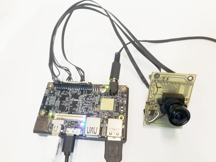
Since the clock frequency of MT9V034 camera is not too high (~27 Mhz), I could easily hook it up to the LS extension connector of the Ultra96 board which you can see in the following image:
Important:
page 8 of the manual indicates that the maximum voltage for the HD IO is 3.3v.
However, in the bord's schematic, the IO bank is connected to the 1.8V rail which puts a limitation of 1.8+0.5V on the maximum input voltage. For a proper connection, one must add a level shifter to convert the voltage levels of the camera.
The design files for the camera breakout board are also open-source and is available here.
SoftwareNow that the hardware is ready and the bitstream is generated, we need to create a Pynq overlay to use it to program the PL within the Pynq environment. To do this, we need the bitstream and a.tcl file describing our block design. These two files should be exported through the File->Export->Export Block Design/Bitstream File. Next, we must rename these two files to an identical name and put them on an arbitrary location of the Pynq filesystem.
Now, we need to open the jupyter notebook on the board and load PL with the newly created overlay:
Next, we need to configure the color convert and pixel pack IP blocks. Since the output of camera color interpolation is a 24-bit RGB video, we need to set the pixel pack to 24. Furthermore, I've set the color conversion matrix to 0.5 to simultaneously convert the RGB image into grayscale and also apply a little bit of digital gain ( Otherwise, I should have chosen 0.33 instead of 0.5). This is done as follows:
For configuring the AXI Stream switches, I wrote two functions for choosing one of the two possible pipelines, one with edge detection IP and the other without it. This is done as follows:
Now that the pipeline is configured, we're ready to read the camera frames using the VDMA. To do this, we need to configure the DMA accordingly:
We're now continuously reading frames from the camera and storing them into the DDR video framebuffer. We can use the pyplotlib to plot one of these frames in the Jupyter notebook:
We can also configure the Display port of the Ultra96 to output a live video of these frames. To do so, we use Pynq's DisplayPort driver. First, we should configure the driver:
The monitor should turn black now which means we're ready to copy the camera frames onto the monitor:
And finally, here is the video showing the results:
SummeryIn this blog, we made a simple project to do hardware-accelerated image processing using Xilinx Zynq FPGAs and Pynq. This blog was the second in the Embedded Systems for Robotics blog series where I demonstrated the flexibility and power of FPGAs for robotics. The image processing task we accelerated in this post was somewhat useless but, the core idea is the same for bigger projects. For example, feature-based SLAM algorithms require feature extraction from the images to construct the visual geometry pipeline which can be easily done in hardware. Furthermore, in AI perception pipelines, there are preprocessing computations on the image which also may be easily handled by the hardware.


Comments
Please log in or sign up to comment.