


Hardware components | ||||||
 |
| × | 4 | |||
 |
| × | 4 | |||
 |
| × | 4 | |||
 |
| × | 1 | |||
 |
| × | 4 | |||
| × | 1 | ||||
| × | 4 | ||||
_ztBMuBhMHo.jpg?auto=compress%2Cformat&w=48&h=48&fit=fill&bg=ffffff) |
| × | 1 | |||
Software apps and online services | ||||||
| ||||||
 |
| |||||
There are three parts to this project series.
- Part 1: Making the Simon Says Game
- How to set up a project in Upverter
- How to lay out a PCB in Upverter
- How to to draw traces on a double sided PCB in Upverter
- How to fix issues in Upverter
- Which files to export from Upverter and how to export them
For our first PCB design ever, we started with Katie's version of the classic Simon Says game. You can find the project and code for this Simon Says game here.
Katie laid out her hardware schematic in Fritzing. Fritzing has its own free PCB creation tool, but we decided to go with Upverter, since it's a bit more powerful and everyone we talked to said it was better.
Upverter - Setting upUpverter is a great tool with lots of advantages, but like any new software there is a lot to learn. You can check out a library of video tutorials that will help you along the way here.
For this project Katie created the schematic and Monica did the PCB layout. Katie will walk you through the steps to create the schematic below and Monica will explain the PCB layout. If you want to go straight to our final design, you can find it here.
Setting up your project:
Create your Upverter account. Go to Hackster Apps, find Upverter, and click the yellow "Try it now" button.
We started with an Arduino Shield created by Upverter here. Click on the “fork” button on the top right of the screen. This allows you to copy the design and use it in your own design.
Name your project and change any other settings you wish. Hit Save.
Click the blue “Open Editor” button in the left corner of the screen. You are now ready to start creating your schematic!
Updating your Arduino Shield:
- You’ll notice in the schematic, the Arduino shield parts are yellow. In Upverter, if a part has been updated it will turn yellow. Double click the top Molex 90120-0768 part and click “Update”.
- You'll see a lot of red, don't worry we will fix this in the following steps.
- Flip the part so that the pins are facing to the left in your schematic. Do this by clicking on the part and clicking the “flip” button on your task bar.
- There are still some errors (red dots/lines). The nets on these pins are only there to show which pins on the shield match with the pins on the Arduino. I chose to delete the nets and label each pin using annotations instead.
- Delete the nets by clicking a net and clicking the trash can in the task bar (You can click and drag your mouse to highlight more than one net at once and make this go faster).
- Add annotations by clicking the "T" button on the task bar and typing the pin name (e.g. AREF for pin 1) You can move annotations around the screen by clicking and dragging.
- Repeat steps 1-3 with the bottom Molex 90210-0768 part.
- Update and flip both Molex 90210-0766 parts. You can leave the flags on these parts since they are relatively neat and organized.
- You’ll notice that there is a red error sign on the top part. You can fix this by rearranging or deleting the nets and re-connecting both pins 4 and 5 to the ground symbol. This tutorial explains connecting parts using nets.
- Drag each part toward the corner of your screen so you have a lot of space to place your board components.
Searching for your components:
For our PCB we knew that we wanted to use the same components that we used with our breadboard. We wanted all through-hole (TH) components rather than surface mount (SMD) and we needed the following components
- 4 12mm buttons from sparkfun
- 4 5mm LEDs
- 4 Generic 330 ohm resistors
- 4 Generic 10K resistors
- CEM-1203(42) piezo buzzer.
Follow the steps below to find and place components in Upverter:
- Click the components button in the task bar.
- In the search bar, type your part number or the name of the part you want.
- Make use of the filters on the left hand sidebar. Choose parts that include a footprint so that your part shows up in your PCB layout and you do not have to create your own later.
- When you’ve found the part you want click the “place component” button. This will bring you back to your schematic and let you place as many of the components you need for your layout.
Learn more about adding components to your design here.
Once you find and place your components, complete the following steps:
- Add annotations to each button and LED indicating the color that each corresponds to so you can match the correct colors with the correct pin numbers on your shield.
- Double click on the resistor and change the “??” to 10K for each button resistor and 330ohm for each LED resistor.
- Connect all components to power and ground using nets.
- Place a “no connect” flag (the x symbol) on any pin that is not connected. (This is not necessary, but helps to easily show what is and isn’t connected).
Our final schematic layout for our Simon Says game shield looks like this:
Nice work on the schematic!
- Now open the PCB Layout tab in Upverter.
You should see a bunch of parts, plus mess of green lines, or ‘rats nests,’ between the unconnected traces. These are based on the connections we made on our schematic in the previous step. These handy lines will guide us when we draw our traces.
- The first thing to do is drag the components onto the shield and lay them out in a way that makes sense.
This part can be kind of a puzzle. You need to make sure that traces will be able to run far enough apart without crossing or running under your components. There are options to turn the part clockwise or counterclockwise.
You can also flip parts to the other side of the board by selecting the 'flip' tool, but be careful with this! See the yellow parts on the board below? Those are flipped and show up on the other side of the board. This isn't a problem for parts that don't have specific power and ground pins, like resistors, but for many components you will need be aware of the orientation of your final parts on your board. Notice the yellow LED below? We later flipped this back to the front so our LEDs were all oriented the same way in our layout.
The board components are all laid out, but we still have to draw the traces.
- Open the trace tool.
If you’ve looked closely at PCBs, especially older PCBs, you’ve probably noticed that traces often have 45 degree angles at the bends:
Why are 45 degree bends used? Previously, the machines that made the traces only had 8 directions they could travel in, so they weren’t able to just draw straight lines from one area of the board to another. They could only go horizontal, vertical, and at 45 degrees. People still use them because of tradition, and they they look kind of neat. Upverter lets you draw 45 degree angles just by clicking and dragging the tool. Just click and drag between components, following the rats nest lines.
- You can change the width of the traces by selecting them and changing the width in the trace inspector.
One thing to make sure you don’t do is cross traces. In the image below, you’ll see that there’s a trace that crosses over the other traces. All the traces that are connected to these ones incorrectly now have a reddish outline.
- Delete the bad traces and reroute them so they don't cross.
Problems will also show up under the 'constraints' tab in the sidebar. This is a great place to see if your traces are too close together, or crossed. You can choose to ignore them if you know they won't be an issue.
Making a double sided PCBThis PCB needs to be double sided because there’s no easy way to not cross the traces here unless we do them on the bottom side.
- Select “HIDE ALL” on top layer on the layers tab.
- Now you can start routing the bottom layer. The traces drawn on the back side of the board will show up as light blue instead of green.
Want your traces to be straighter? Try using snap to guides or snap to grid at the bottom. You can toggle between the two. You can also change the size of the grid.
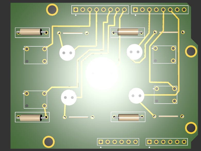
Here's what we end up with:
Zak Homuth from Upverter was kind enough to review it, and he added a ground pour, since that's a best practice. It's always good to get a few people to review your PCB before your send it in to be produced.
At this point, our PCB is ready to be sent off for production! All you have to do is go to "Project" > "Export files" and download the Gerber files.
Depending on who is manufacturing your board, they might need the files in a different format. Some manufacturers also need the layout to be done in a particular way - for instance, traces of a specific width.
Of course, you can always manufacture the PCB yourself, which is what we'll be covering in our next tutorial, Breadboard to PCB 3 - Manufacturing the PCB.


_3u05Tpwasz.png?auto=compress%2Cformat&w=40&h=40&fit=fillmax&bg=fff&dpr=2)

Comments
Please log in or sign up to comment.