Using Xilinx's board to design Fully Connected Network core can be easy. But to utilize this core in order to use it in DNN calculation is another thing. This project mainly focuses on designing AI accelerator using Xilinx's CDMA to load weight and input to Block Ram of PL region.
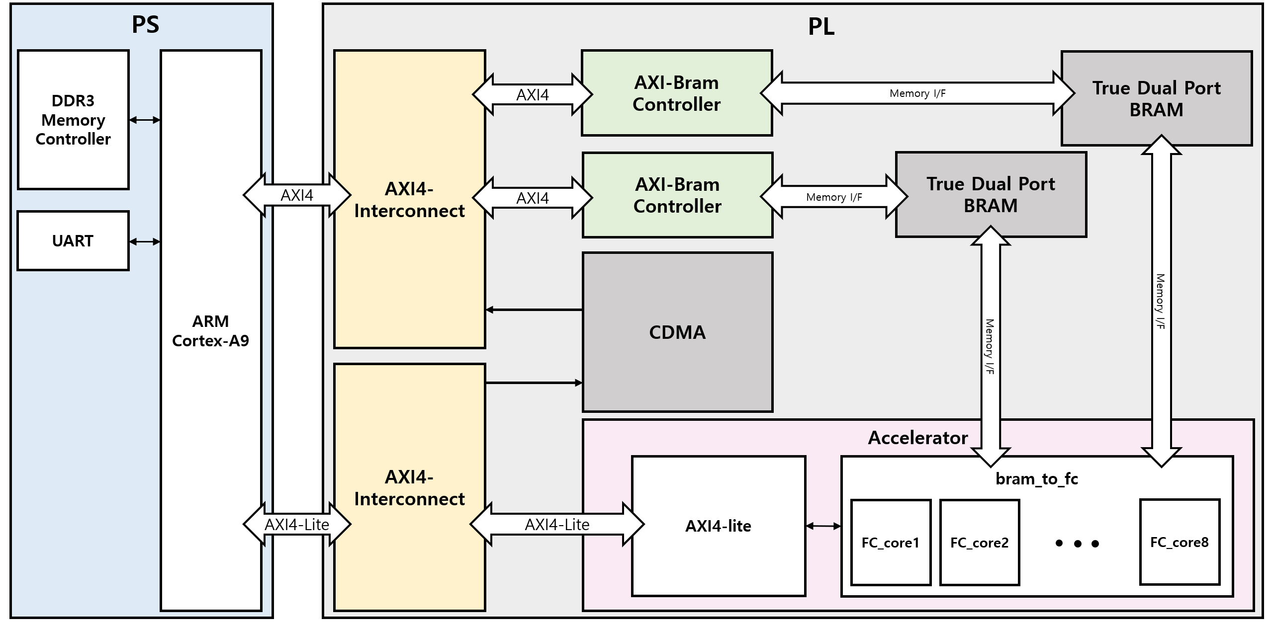
SchematicFirst We created a schematic of whole system. There are two Bock ram in order to store input feature and weight data, respectivly. Each block RAM is connected to a CDMA block, allowing the DRAM to access the Bram. Each Block RAM is also connceted to main accelerator that is consisted of 8 FCN cores and FSM to controll cores's operation.
The full activation seqeunce follows
- Store feature and weight in DDR memory.
- Send these data to block ram1 and block ram2 using CDMA, respectivly.
- Send activate signal to FC core in order to proceed FCN calculation.
- store result in blcok ram.
- repeat this procedure until the first layer forward pass is done.
- repeat whole procedure with chaing input to result stored in block ram.
To use direct memory access, we used cdma. You can refer to xilinx turoial at XIinx website. And we used Xilinx Vivado, version 2021.1, which you can download at the Xilinx website.
First, configure the processor to enable S_AXI_HP0 interface.
Second, add cdma and bram module. Vivado connect cdma and bram to processor by Run Connection Automation. Then the design should look similar to the figure below.
Accelerator IP is consisted of 4 source files.
Accelerator : It connects AXI4-lite module and bram_to_fc module.
AXI4-lite : It performs AXI4-lite interface to transfer result value from PL to PS. And it transfers fsm signal to bram_to_fc module.
bram_to_fc : It recieves feature map and weight from bram0, bram1 and sends them to sumproduct_core.
sumproduct_core : It performs sumproduct calculation with 8bit input. and returns 32bit output.
We created AXI4 peripheral to make AXI4-lite template. Interface type is lite and we made 10 registers. Then we modify template to make AXI4-lite module.
We added 4 Verilog files to generate Accerelator IP.
Then we used VIVADO block digram tool to construct whole design. We used dual port bram with 64bit data width to maximize the efficency of system.
At address editor we changed axi_bram_ctrl range from 8k to 64k.
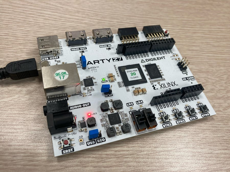
We tested our accelerator on Arty Z7-20, we export our hardware to VITIS. To test our accelerator performences, we compared same task run time between SW and HW.
HW runtime: data send time + HW calcuation time + data receive time
SW runtime: SW calcuation time
1. Transfer feature map and weight from DDR3 to BRAM using CDMA.
//transfer feauture map from DDR3 to Bram0
XAxiCdma_IntrEnable(&xcdma, XAXICDMA_XR_IRQ_ALL_MASK);
Status = XAxiCdma_SimpleTransfer(&xcdma, (u32)source_0, (u32) cdma_memory_destination_0, numofbytes, Example_CallBack, (void *) &xcdma);

//transfer weight from DDR3 to Bram1
XAxiCdma_IntrEnable(&xcdma, XAXICDMA_XR_IRQ_ALL_MASK);
Status = XAxiCdma_SimpleTransfer(&xcdma, (u32)source_1, (u32) cdma_memory_destination_1, numofbytes, Example_CallBack, (void *) &xcdma);
2. Send FSM run signal and number of inputs that you want to transfer.
Xil_Out32((XPAR_ACCELERATOR_0_BASEADDR) + (CTRL_REG*4), (u32)(numofbytes | 0x80000000));3. Check result of HW calculation.
OT_RSLT_HW[0] = Xil_In64((XPAR_ACCELERATOR_0_BASEADDR) + (RESULT_0_REG*AXI_DATA_BYTE));
OT_RSLT_HW[1] = Xil_In32((XPAR_ACCELERATOR_0_BASEADDR) + (RESULT_1_REG*AXI_DATA_BYTE));
OT_RSLT_HW[2] = Xil_In32((XPAR_ACCELERATOR_0_BASEADDR) + (RESULT_2_REG*AXI_DATA_BYTE));
OT_RSLT_HW[3] = Xil_In32((XPAR_ACCELERATOR_0_BASEADDR) + (RESULT_3_REG*AXI_DATA_BYTE));
OT_RSLT_HW[4] = Xil_In32((XPAR_ACCELERATOR_0_BASEADDR) + (RESULT_4_REG*AXI_DATA_BYTE));
OT_RSLT_HW[5] = Xil_In32((XPAR_ACCELERATOR_0_BASEADDR) + (RESULT_5_REG*AXI_DATA_BYTE));
OT_RSLT_HW[6] = Xil_In32((XPAR_ACCELERATOR_0_BASEADDR) + (RESULT_6_REG*AXI_DATA_BYTE));
OT_RSLT_HW[7] = Xil_In32((XPAR_ACCELERATOR_0_BASEADDR) + (RESULT_7_REG*AXI_DATA_BYTE));

for (ii=0; ii<8; ii++){
    			printf("%d \n", OT_RSLT_HW[ii]);
    		    }
4. Check result of SW calculation.
You can see board test result below.
As we can see in this result the time usage of our accelerator was much lesser(11.40+13.44+4.71micro seconds) than comparson done on PS region(104.99mircro seconds).


Comments
Please log in or sign up to comment.