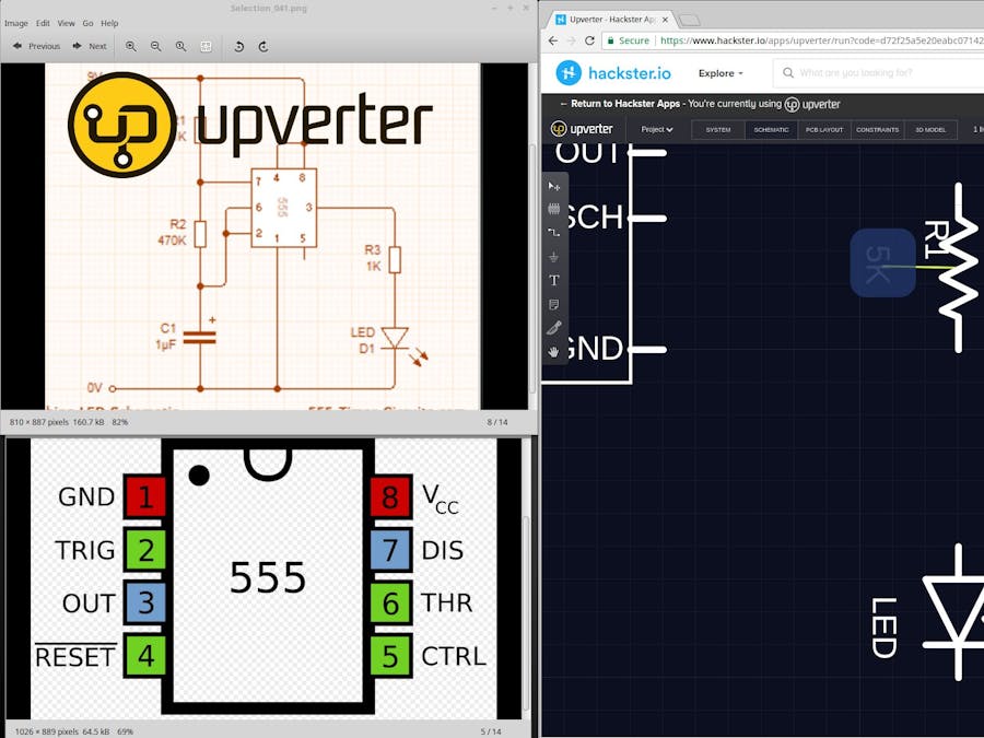
Hello, everyone. I've been thinking a bit about how to design a PCB as a non-electronics-expert, and because in the Hackster Live Meetup we do not have much time, I decided to elaborate this tutorial that will serve as reference for this month's challenge. It is based on the famous IC 555 which is very versatile and together with a few other components, it will serve us to develop our "Hello World PCB".
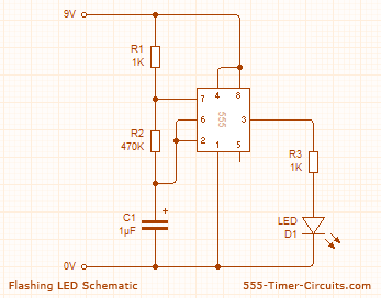
First we must get the schematic of the circuit, which is called "Flashing LED" and we can download it from the following page www.555-timer-circuits.com
In that same page you will find a video of how to assemble the circuit and it would be highly recommended to make it; it will serve you a lot when creating the PCB.
We also need to share the IC 555 Datasheet or an image of the pinout:
If you do not have the electronic components, you can use a simulator, such as https://circuits.io.
Well, we already have what it takes to start creating our PCB, which we will do in the following steps:
1. Create or log in to a Hackster.io account.
2. Select in the Apps menu the Upverter option.
3. Open the Upverter Dashboard.
4. Create a new project.
5. Place the components in the schematic and join them.
6. Go to the option PCB Layout to create the PCB and organize the components, and then create the tracks that will join them electrically.
7. Generate the gerber to send them to the manufacturer.
I know, it seems complicated, but believe me, it is not and you will have so much fun.
Are you ready? Let's start!
1Create or log in to a Hackster.io account.
Select in the Apps menu the Upverter option.
Open the Upverter Dashboard.
Click on the Upverter logo.
Create a new project.
Once you finish filling out the form and click on the create button, the main schematic screen will be displayed.
Place the components in the schematic and join them.
Now the fun part begins. To start placing the components we need to have a list of all the parts; this will save us a lot of time.
Upverter offers several options of components to add. It has a database with more than 1M of components, and if it does not exist, it gives you the option to create it for you (for a fee). Besides that, Upverter offers a catalog of generic components to save time when adding common components to your design, like resistors and capacitors. Generics allow you to specify the parameters you care about (value, tolerance, etc.) and select a standard footprint, without having to select an orderable manufacturer part number just yet.
I will not go into this topic further, but if you want more information, you can access the Upverter resource center: https://upverter.com/documentation/
Next, I will show you how to add a generic component and one already defined in Upverter.
Generic Component
Oops! I forgot - you can use keyboard shortcuts for these and many other options. To access them, single click on the icon with the question mark.
Now it's up to you to practice, add 1 capacitor and play with the options of this bar, copy, paste, flip, etc.
Change Values in Generic Components
This is one of the advantages of the generic components: you can change their values and type of footprint. A footprint or land pattern is the arrangement of pads (in surface-mount technology) or through-holes (in through-hole technology) used to physically attach and electrically connect a component to a printed circuit board (Wikipedia).
To change the values of the component, double click on the component, and in the popup window change the following values:
- footprint type: None to Axial
- resistance: 5K to 1K
Default Component
This type of component, unlike generic, its values are already defined and can not be modified, unless a copy is made, which will generate a new component with the new values defined by you.
These are the predefined components that must be included:
- 5mm Green LED (Diffused) --- Lite-On --- LTL2R3KG
- 555 Timer/Oscillator IC --- Texas Instruments --- NE555P
- Terminal block, 2 positions --- On Shore Technology --- OSTTE020104
The predefined components can be searched by their description or part number.
We only have to add two new symbols, VCC and GND. For them we select the Connection Maker toolbar and we add them.
We have everything ready to start ordering and counting all the parts. For this there is no single method or a magic recipe (in PCB crafts). The schematic and common sense will help us to achieve this, and of course we will have fun along the way. If you want to move to the other level you can download this excellent book that gives us SEEED STUDIO.
Connecting Parts Together
I'm not going to entertain this much here. The guys of Upverter have made an excellent video that I recommend you watch, and below are some images of how I did it.
Note: I want to add something that I did not see in the video, and it is the following: when the network has 3 elements or more, you must give it a name. The App indicates by highlighting it and marking it as a violation of the constraints. So, to give it a name just double click on it and write the name (whatever you want).
Go to the option PCB Layout to create the PCB and organize the components, and then create the tracks that will join them electrically.
If you think you've had a lot of fun so far, wait, there's still more! The time has come to accommodate all the components on a PCB. Just like in the previous step, the guys from Upverter have an excellent video that will explain to you in detail how to do it.
Some pictures of how I did it.
Using Layers
Our PCB has arranged all its parts in layers, like an onion, and to use them is very simple. In the toolbar on the right, click LAYERS. Then click on the HIDE ALL button.
Hey! Where are the components? :) Do not worry, there they are, just hidden. To make them visible again, click the SHOW ALL button.
Now, it's up to you to practice, OFF and ON, each of the layers to recognize them.
Note: Not all layers are in use or have components to display, so do not worry that nothing appears on the screen.
Copper Pour
In electronics, the term "copper pour" refers to an area on a printed circuit board filled with copper (the metal used to make connections in printed circuit boards). Copper pour is commonly used to create a ground plane (Wikipedia).
We will start with the back of the PCB and then with the front.
It's up to you to practice. Click on the "Top Copper" layer and create the copper plane for the front of the PCB.
Add Images and Text
This option is one of those things that I like most about Upverter, because it offers a very simple way for you to add text and images to the PCB, something that is complicated in other programs for PCB design (Eagle, Kicad, etc).
We can put the text or image on either side of the PCB or both. Each side is identified as: Front = Top Silkscreen; Back = Bottom Silkscreen.
Add Text
To add text to your PCB, do the following:
Add Image
Before adding an image, it is highly recommended that you have converted to monochrome, and with a good resolution.
Now it's up to you - put an image on the back of the PCB. Some tips:
- Hide all layers
- Activate only the back layers
- Select the layer "Bottom Silkscreen"
Repeat the above steps. And don't forget to have fun!
Generate the gerber to send them to the manufacturer.
The time has come for the truth. Once you have double checked your work, you must generate the gerbers to send them to the PCB dealer. There are many options. I will use OHSPark since its service supports 100% Upverter. Also, that purple color, it's super cool!
Generate the Gerber
Send to OSHPark
That's all folks. You have finished creating your PCB using the Upverter App. It really is my wish that this tutorial has been useful for you. Please do not forget to comment that you liked it, click "Respect project" and share.
New videos


_3u05Tpwasz.png?auto=compress%2Cformat&w=40&h=40&fit=fillmax&bg=fff&dpr=2)

Comments
Please log in or sign up to comment.