


Hardware components | ||||||
 |
| × | 1 | |||
 |
| × | 1 | |||
Software apps and online services | ||||||
| ||||||
Introduction
The Inter-IC Sound Interface (I2S for short) was developed by Philips to transmit digital audio data via a serial interface between different ICs (e.g. from a processor to a DAC). The interface uses the following signals for data transmission:
- SCK (Serial clock) - Clock line for data transmission.
- SD (Serial data) - The individual bits of each data word are transmitted via this line.
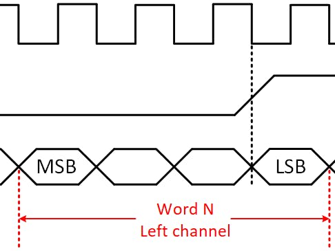
- WS (Word select) - Defines the length of the transmitted data word. It is used to mark the right or left audio channel.
Only audio data is transmitted via the I2S. Additional data, such as the configuration of individual bus users, are transmitted via other interfaces. A data transfer always takes place in one direction and between two bus users, whereby the bus user must act as a master and is responsible for generating the clock signals. In complex systems consisting of several transmitters and receivers, the clock signals are generated by an external bus master and the respective transmitter generates the data.
All data are transmitted as two's complement and MSB First. If there is a positive difference in the word widths of the receiver and transmitter (i.e. if the word width of one participant is smaller than that of the other), the remaining bits are filled with 0. If the difference is negative (ie the word width of one participant is larger than that of the other), the remaining bits are ignored. According to the specification, the data can be synchronized to the positive or the negative clock edge, whereby the data is always read in with the negative clock edge.
The WS signal selects the active channel and all data within a low or high phase are assigned to the respective channel. The following applies:
- WS = 0 – Channel 1 (Left)
- WS = 1 – Channel 2 (Right)
The WS signal must always be changed one clock cycle before the MSB of the next data word so that the receiver can read the data into the correct channel. The clock frequency of the WS signal usually corresponds to the sampling frequency of the audio signal.
In the first part, I would like to show how a simple I2S transmitter can be designed and used to output a constant sound via a loudspeaker using a CS4344 stereo D/A converter.
The sound to be output is to be stored in the block memory of the FPGA and read out by the transmitter which sends the data to the D/A converter. The entire project is divided into three sections, which I will discuss gradually:
- A Top design which integrates the system clock and an I2S module
- The I2S module which integrates the ROM and the I2S transmitter
- The I2S transmitter
The bottom end of the design should be the I2S transmitter, which has the task of sending the individual data words over the I2S interface.
The block diagram results in the following entity of the transmitter:
entity I2S_Transmitter is
    Generic (   WIDTH   : INTEGER := 16
                );
    Port (  Clock   : in STD_LOGIC;
            nReset  : in STD_LOGIC;
            Ready   : out STD_LOGIC;
            Tx      : in STD_LOGIC_VECTOR(((2 * WIDTH) - 1) downto 0);
            LRCLK   : out STD_LOGIC;
            SCLK    : out STD_LOGIC;
            SD      : out STD_LOGIC
            );
end I2S_Transmitter;
The size of a data word is defined via the parameter WIDTH.
A three-stage state machine controls the transmitter and is described as follows:
architecture I2S_Transmitter_Arch of I2S_Transmitter is

    type State_t is (State_Reset, State_LoadWord, State_TransmitWord);

    signal CurrentState     : State_t      := State_Reset;

    signal Tx_Int  : STD_LOGIC_VECTOR(((2 * WIDTH) - 1) downto 0)  := (others => '0');
    signal Ready_Int        : STD_LOGIC    := '0';
    signal LRCLK_Int        : STD_LOGIC    := '1';
    signal SD_Int           : STD_LOGIC    := '0';
    signal Enable           : STD_LOGIC    := '0';

begin

    process
        variable BitCounter : INTEGER := 0;
    begin
        wait until falling_edge(Clock);

        case CurrentState is
            when State_Reset =>
                Ready_Int <= '0';
                LRCLK_Int <= '1';
                Enable <= '1';
                SD_Int <= '0';
                Tx_Int <= (others => '0');
                CurrentState <= State_LoadWord;
            when State_LoadWord =>
                BitCounter := 0;
                Tx_Int <= Tx;
                LRCLK_Int <= '0';
                CurrentState <= State_TransmitWord;
            when State_TransmitWord =>
                BitCounter := BitCounter + 1;
                if(BitCounter > (WIDTH - 1)) then
                    LRCLK_Int <= '1';
                end if;
                if(BitCounter < ((2 * WIDTH) - 1)) then
                    Ready_Int <= '0';

                    CurrentState <= State_TransmitWord;
                else
                    Ready_Int <= '1';

                    CurrentState <= State_LoadWord;
                end if;
                Tx_Int <= Tx_Int(((2 * WIDTH) - 2) downto 0) & "0";
                SD_Int <= Tx_Int((2 * WIDTH) - 1);
        end case;
        if(nReset = '0') then
            CurrentState <= State_Reset;
        end if;
    end process;
    Ready <= Ready_Int;
    SCLK <= Clock and Enable;
    LRCLK <= LRCLK_Int;
    SD <= SD_Int;
end I2S_Transmitter_Arch;
During a reset, the output signals are deleted and the clock for SCLK is deactivated. After the reset, the machine changes from the State_Reset state to the state State_TransmitWord. In this state, the machine transmits the content of the buffer Tx_Int via the I2S interface.
As soon as the transmission of the last data bit is started, Ready is set to signal the end of a transmission and the readiness to accept new data. The machine then changes to the state State_LoadWord state, where the send buffer is filled with a new data word and a new transfer is started.
The I2S module
The I2S transmitter is used by the higher-level I2S module to transfer data from a ROM to the D/A converter.
With the following entity:
entity I2S is
    Generic (   RATIO   : INTEGER := 8;
                WIDTH   : INTEGER := 16
                );
    Port (  MCLK     : in STD_LOGIC;
            nReset   : in STD_LOGIC;
            LRCLK    : out STD_LOGIC;
            SCLK     : out STD_LOGIC;
            SD       : out STD_LOGIC
            );
end I2S;
The parameters RATIO and WIDTH define the ratio of SCLK to MCLK and the width of a data word per channel.
In addition to the I2S transmitter, the module uses a ROM, which can be created via the block memory generator and filled with data. Both can be done using Vivado's IP integrator.
Finally, the ROM is initialized with a sine signal coe file (see attachments) via Other Options.
The I2S module uses a state machine to read data from the ROM and transfer it to the I2S transmitter.
architecture I2S_Arch of I2S is

    type State_t is (State_Reset, State_WaitForReady, State_IncreaseAddress, State_WaitForStart);

    signal CurrentState : State_t    := State_Reset;

    signal Tx  : STD_LOGIC_VECTOR(((2 * WIDTH) - 1) downto 0)      := (others => '0');
    signal ROM_Data : STD_LOGIC_VECTOR((WIDTH - 1) downto 0)       := (others => '0');
    signal ROM_Address  : STD_LOGIC_VECTOR(6 downto 0)             := (others => '0');

    signal Ready        : STD_LOGIC;
    signal SCLK_Int     : STD_LOGIC                                         := '0';

    component I2S_Transmitter is
        Generic (   WIDTH   : INTEGER := 16
                    );
        Port (  Clock   : in STD_LOGIC;
                nReset  : in STD_LOGIC;
                Ready   : out STD_LOGIC;
                Tx      : in STD_LOGIC_VECTOR(((2 * WIDTH) - 1) downto 0);
                LRCLK   : out STD_LOGIC;
                SCLK    : out STD_LOGIC;
                SD      : out STD_LOGIC
                );
    end component;

    component SineROM is
        Port (  Address : in STD_LOGIC_VECTOR(6 downto 0);
                Clock   : in STD_LOGIC;
                DataOut : out STD_LOGIC_VECTOR(15 downto 0)
                );
    end component SineROM;

begin

    Transmitter : I2S_Transmitter generic map(  WIDTH => WIDTH
                                                )
                                  port map(     Clock => SCLK_Int,
                                                nReset => nReset,
                                                Ready => Ready,
                                                Tx => Tx,
                                                LRCLK => LRCLK,
                                                SCLK => SCLK,
                                                SD => SD
                                                );

    ROM : SineROM port map (Clock => MCLK,
                            Address => ROM_Address,
                            DataOut => ROM_Data
                            );

    process
        variable Counter    : INTEGER := 0;
    begin
        wait until rising_edge(MCLK);
        if(Counter < ((RATIO / 2) - 1)) then
            Counter := Counter + 1;
        else
            Counter := 0;
            SCLK_Int <= not SCLK_Int;
        end if;

        if(nReset = '0') then
            Counter := 0;
            SCLK_Int <= '0';
        end if;
    end process;

    process
        variable WordCounter    : INTEGER := 0;
    begin
        wait until rising_edge(MCLK);
        case CurrentState is
            when State_Reset =>
                WordCounter := 0;
                CurrentState <= State_WaitForReady;
            when State_WaitForReady =>
                if(Ready = '1') then
                    CurrentState <= State_WaitForStart;
                else
                    CurrentState <= State_WaitForReady;
                end if;
            when State_WaitForStart =>
                ROM_Address <= STD_LOGIC_VECTOR(to_unsigned(WordCounter, ROM_Address'length));
                Tx <= x"0000" & ROM_Data;
                if(Ready = '0') then
                    CurrentState <= State_IncreaseAddress;
                else
                    CurrentState <= State_WaitForStart;
                end if;
            when State_IncreaseAddress =>
                if(WordCounter < 99) then
                    WordCounter := WordCounter + 1;
                else
                    WordCounter := 0;
                end if;
                CurrentState <= State_WaitForReady;

        end case;
        if(nReset = '0') then
            CurrentState <= State_Reset;
        end if;
    end process;
end I2S_Arch;
The first process is used to generate the clock signal SCLK required for the transmitter from MCLK.
process
    variable Counter    : INTEGER := 0;
begin
    wait until rising_edge(MCLK);
    if(Counter < ((RATIO / 2) - 1)) then
        Counter := Counter + 1;
    else
        Counter := 0;
        SCLK_Int <= not SCLK_Int;
    end if;

    if(nReset = '0') then
        Counter := 0;
        SCLK_Int <= '0';
    end if;
end process;
The second process takes care of the processing of the state machine. After leaving the state State_Reset, the machine waits in the State_WaitForReady state until the transmitter signals readiness with the Ready signal.
As soon as the transmitter is ready, the machine changes to the State_WaitForStart state. In this state, the current data word is read from the ROM and transferred to the transmitter.
The ROM is shown here only contains the information from one channel. The data must be expanded accordingly for the second channel.
The ROM is shown here only contains the information from one channel. The data must be expanded accordingly for the second channel.
As soon as the transmitter clears the ready signal and begins transmitting the data, the state machine changes to the State_IncreaseAddress state. In this state, the ROM address is increased by one and then switched back to the State_WaitForReady state
The Top module
The last component is the top design that includes the I2S module and a clocking wizard.
This example uses the following parameters to control the CS4344:
- MCLK: 12.288 MHz
- SCLK: 1.536 MHz
- LRCLK: 48 kHz
- RATIO: 8
- WIDTH: 16
The Clocking Wizard is used to generate the 12.288 MHz clock from the oscillator frequency of the programmable logic. For this purpose, the clocking wizard is inserted via the IP integrator and instantiated together with the finished I2S module in the VHDL code.
entity Top is
    Generic (   RATIO   : INTEGER := 8;
                WIDTH   : INTEGER := 16
                );
    Port (  Clock   : in STD_LOGIC;
            nReset  : in STD_LOGIC;
            MCLK    : out STD_LOGIC;
            LRCLK   : out STD_LOGIC;
            SCLK    : out STD_LOGIC;
            SD      : out STD_LOGIC;
            LED     : out STD_LOGIC_VECTOR(3 downto 0)
            );
end Top;

architecture Top_Arch of Top is

    signal nSystemReset : STD_LOGIC := '0';
    signal MCLK_DCM     : STD_LOGIC := '0';
    signal Locked       : STD_LOGIC := '0';

    component I2S is
        Generic (   RATIO   : INTEGER := 8;
                    WIDTH   : INTEGER := 16
                    );
        Port (  MCLK    : in STD_LOGIC;
                nReset   : in STD_LOGIC;
                LRCLK    : out STD_LOGIC;
                SCLK     : out STD_LOGIC;
                SD       : out STD_LOGIC
                );
    end component;

    component AudioClock is
        Port (  ClockIn     : in STD_LOGIC;
                Locked      : out STD_LOGIC;
                MCLK        : out STD_LOGIC;
                nReset      : in STD_LOGIC
                );
    end component;

begin

    InputClock : AudioClock port map (  ClockIn => Clock,
                                        nReset => nReset,
                                        MCLK => MCLK_DCM,
                                        Locked => Locked
                                        );

    I2S_Module : I2S generic map (  RATIO => RATIO,
                                    WIDTH => WIDTH
                                    )
                          port map ( MCLK => MCLK_DCM,
                                     nReset => nSystemReset,
                                     LRCLK => LRCLK,
                                     SCLK => SCLK,
                                     SD => SD
                                     );

    nSystemReset <= nReset and Locked;
    LED(0) <= nReset;
    LED(1) <= Locked;
    LED(2) <= nSystemReset;
    MCLK <= MCLK_DCM;

end Top_Arch;
The design can now be implemented, transferred to the FPGA and tested. Ideally, the D/A converter outputs a 480 Hz sine signal, since the signal pattern from the ROM has a length of 100 samples and the sampling frequency is 48 kHz. The communication and the signal can be checked with an oscilloscope:
Also, the audio signal can be checked. The FFT function of an oscilloscope is the ideal tool to do it.
In the next part of the tutorial, we will add an AXI-Stream interface to the I2S transmitter and connect it with the Processing System of the ZYNQ to play some audio from an SD card.


Comments
Please log in or sign up to comment.