While my recent ESP32-S Dev Board really does the trick to help my development cycle along, I very quickly ran into another obstacle, in the sense that, after doing stuff on the breadboard, moving those components onto a more permanent location, either as a next stage prototype or more likely that the project is so small and insignificant not to warrant the effort actually to design a PCB for it. This could be rectified by using another one of my recent designs, an SMD breadboard PCB, but that would not always do either.
MakerIoT SMD Prototype development PCB
That got me thinking, and while staring at the ever-present Arduino Uno on its corner of the work-bench, I suddenly remembered that I have once seen an Arduino Prototype Shield, like a plug-on breadboard, with breakouts of all the pins etc… While I do not personally own a lot of commercial Arduino Shields, as I tend to build my own or design a custom-purpose PCB instead, it did not take me long to settle on a new design, that could potentially solve my problem, and hopefully, someone else’s as well…
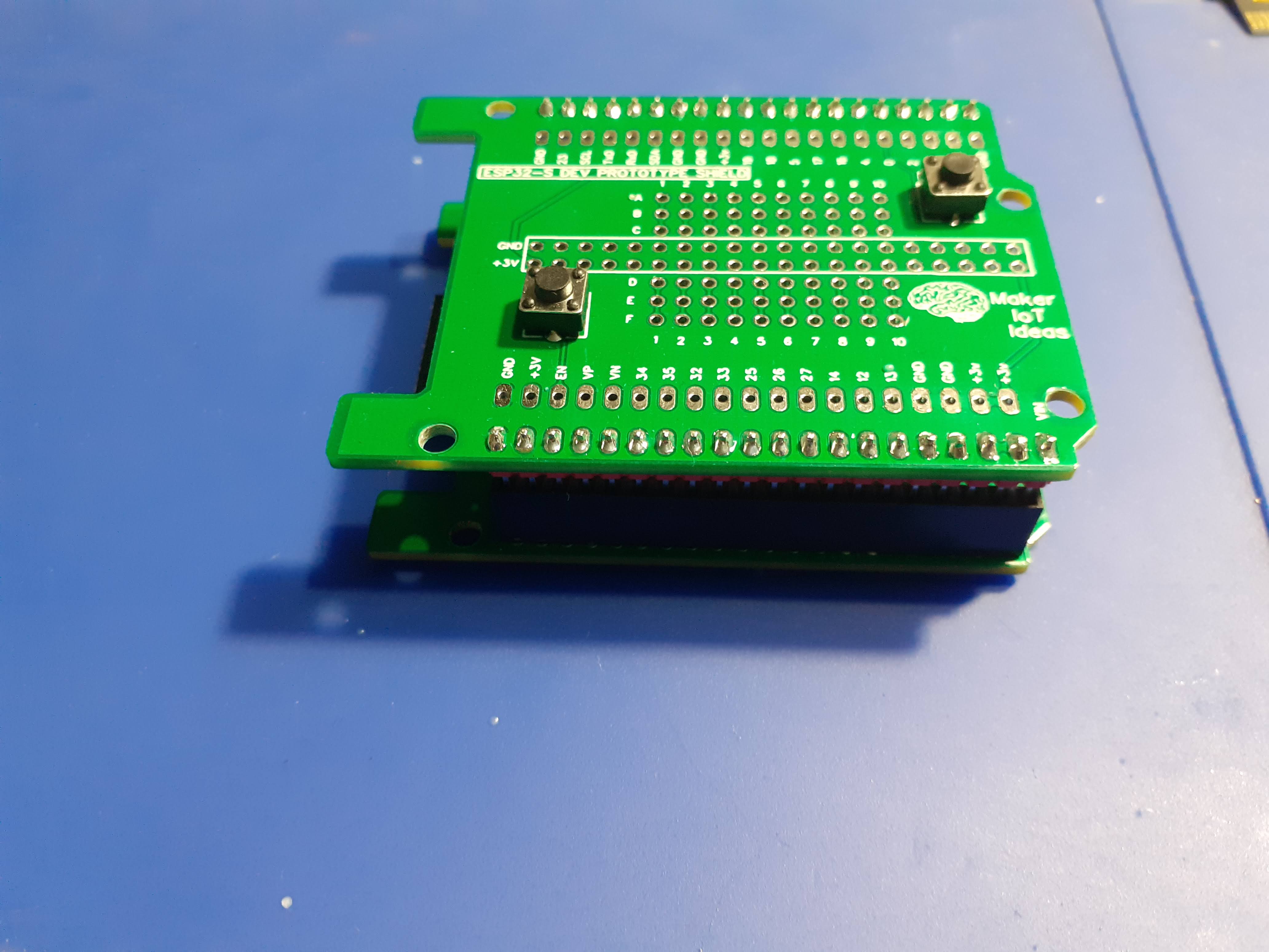
To start off, the PCB is in the same form factor as the ESP32-S Dev Board, namely the Arduino Uno form factor. There are however a few changes, mainly in the number of pins in the headers. This is mainly to accommodate as many of the ESP32-S’s gpio’s as possible. ( Actually, they are all broken out, EXCEPT for the 6 gpio’s that are usually used with the internal Flash memory.)The PCB is designed to be stacked either on top of, or even below, the ESP32-S Dev Board, depending of course on the type of headers that you decide to solder onto the PCB. In order to make connecting to the gpio pins easier, each header row is in fact a double row, with solderable pads in parallel for each gpio on the header row. Flash and Reset buttons are available on top of the shield, they can be fitted of left off, depending on personal preference, as well as how the shield will ultimately be used. The prototyping area in the centre has been slightly reduced from the standard 5-pin-spacer-5-pin column of the traditional breadboard to a 3-pin-gnd-3v-3-pin column layout. the prototyping holes are at a standard 0.1″ or 2.54mm pitch. In total, 60 prototype holes, divided into rows of 10, 3 columns deep, are provided, labelled A-F and 1-10.3.3v and ground are provided in the centre-two rows, to make power easily accessible.
ESP32-S Dev Prototype Shield – Back
The PCB DesignAs this design is basically just two rows of header pins, with a few switches, and a big unconnected prototype area, I did not bother to do a formal schematic for this PCB, but instead jumped straight into the PCB design software and manually designed and routed the tracks and pads that make up this shield.
Note that there are big copper pours on both top and bottom layers, in an attemp to reduce electrical noise and provide better shielding.
ManufacturingThe PCB for this project has been manufactured at PCBWay.Please consider supporting them if you would like your own copy of this PCB, or if you have any PCB of your own that you need to have manufactured.You can get your own copy here


Comments