In many of these projects we focus on what goes into the FPGA or the SOC, for example we have created image and signal processing examples.
However, to be able to use the design we have created we need a board which contains the FPGA / SoC and associated support infrastructure such as memories, clocks, power and interfaces.
In this project we are going to look at the process for designing a board which contains these interfaces based around a SoM. Our target SoM will be the Kria SoM although the process we are taken can be used for other SoM such as the UltraZed, Snickerdoodle, and MicroZed. It can even be used for the design of a chip down solution although that would require a lot more analysis.
The objective of this project is to show the process of designing a SoM based approach. I intend when I a little free time to go away and create the board designed in this project just as I did with the Ultra96V2 breakout and the Smart IoT board.
ProcessOne of the things many companies and people get wrong when developing systems is they rush to the focus on the fun and exciting bit of the project e.g the creation of code, drawing schematics and CAD design of enclosures.
One of the guiding principals of systems engineering is the V Diagram. The V Diagram allows us to decompose and define the system as we work down the V and integrate and test the system as we work up the V.
To implement a V diagram succesfully we need to define and engineering process which runs from beginning enabling all of the relevant stages. We could write several projects on systems engineering alone, so for this project we will keep and process pretty simple.
A typical engineering process to develop a electronic board will go through the following stages
- Problem / Opportunity - In this stage we define the concept - what are we trying to achieve, what is the product and what is the market size for the product.
- Mission Analysis - Is there a business case for this development, what are the costs involved, what regulations need to be followed and how long will it take to return the investment and make a profit. Who are the competitors and how does our product differentiate from it.
- Stake Holder Needs & Requirements - The requirements define the actual functional and non-functional requirements. Functional requirements will include things like interfacing, algorithms to be implemented and sensors to be driven. While non functional requirements will include aspects such as the operational temperature range etc. It is common in the requirements stage to also allocated requirements to particular elements of the system e.g. hardware / FPGA / SW. It is also common to create what is called a compliance matrix which defines if the design will comply with the requirement, assign a technical risk and provide justification for why the design is compliant. Compliance matrixes can be great for identifying technical risk on a project.
- Architecture & Design Solution - The architecture is the first step of converting the requirements for the system into a realized solution. At a fundamental level an architecture is the joining of form to function. An architecture needs to describe the functions that the system will perform (defined in the requirements) and the elements of form that will implement those functions. We may have several different architectures for example the overall system architecture, the electronics architecture which defines the hardware solution and FPGA architecture which defines the functionality contained within the device. This will also include any engineering budgets, derived from the requirements for example power, and mass etc.
- Implementation - This is where the detailed design engineering begins, it is where we created the detailed designs for the hardware and FPGA/SW etc. In this stage we will be creating things such as schematics, layout, RTL and SW code. We will also be doing the design analysis which might be required such as signal and power integrity, part stress analysis, Failure Effects and Criticality Analysis along with the documenting the detailed design so we have a reference.
- Integration, Verification and Validation - During this stage we are verifying the design and demonstrating it achieves the requirements placed upon it. Even though verification comes later in the process we need to consider it from day one. Once the requirements are completed we should create a verification cross reference matric which defines how each of the requirements will be verified. Is it by Test, Analysis, Read Across etc. This VCRM then enables the creation of the test requirements and identifies any test equipment and specialist or custom test equipment required. THINK about this from day one especially on more complex projects, it is not unusual to have a team of engineers developing the test equipment.
Between each of these stages there should be a review against a review check list to check the maturity to progress to the next stage.
Problem OpportunityThe opportunity for this development is a Kria based break out board which provides more generic interfacing than is available on the current KV260 and KR260 boards. This board would enable engineers to develop a wider range of Kria based solutions but providing FMC or SYZYGY interfaces to support a range of different prototyping options. This card is certainly something my company could do with to support several of Kria based solutions currently on going.
Mission AnalysisThis board would enable a range of FMC cards to be connected to a Kria SoM enabling a wider range or prototyping to be undertaken. This would also enable technical risk to be reduced, it would also enable potentially depending upon the cost of the produced board a product which could be sold. The design would also be made open source to people interested in modification or manufacturing themselves.
RequirementsCapturing requirements is always a challenge and doing it in the right tool is also important. For requirements and systems engineering I use enterprise architect which is moderately priced, you can use excel spreadsheets and drawing programs also for the architecture phase.
Writing clear and concise requirements a simple set of rules are followed. Requirements should therefore comply with the following
- Necessary – Success cannot be achieved without these requirements
- Verifiable – You must be able to ensure the requirement can be implemented via inspection, test, analysis or demonstration
- Achievable – Technically possible, with the constraints
- Traceable – Can be traced to from lower level requirements, traces to higher level requirements
- Unique – Prevents contraction between requirements
- Simple and Clear – Each requirement specifies one function
Language used to identify requirements needs to be clear and concise
- SHALL – Denotes a mandatory requirement
- WILL – Denotes the purpose of the part or system
- SHOULD – Denotes a non mandatory requirement
The requirements for this board are as follows
These requirements can be converted to a requirements view which shows not only the requirement but also the difficulty
With the requirements defined we can work on the architecture of the solution.
A simple summary of the requirements is they define a carrier card which provides, UART, JTAG, USB2.0 / 3.0, Ethernet, FMC, with configuration modes selectable and support for SD Card boot.
ArchitectureThe first part of the architectural design is to break down the requirements into a series of functional blocks. As I pointed out above this implements the function and form.
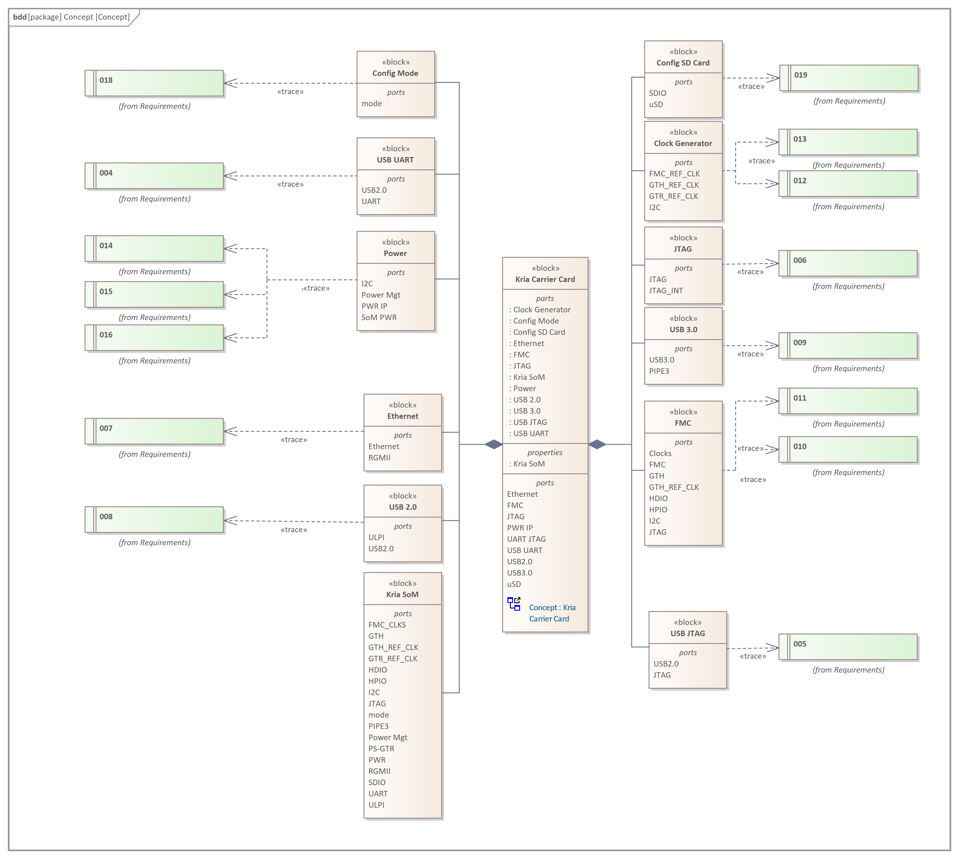
The first step in the process for this is to create a high level diagram which shows which blocks are needed in the design. These blocks should be able to be traced back to the requirements.
Within these blocks we can also define the interfaces which are needed for each block e.g. ULPI, RGMII, etc
Once the high level architecture is completed we can define the lower level architecture and the interfaces which connect from the Kria SoM to the outside world and across the functional blocks. This provides us the ability to begin to think about how we will configure the Kria SoM.
With the architecture defined the next step is to start the detailed design. Of course, for this project we need to create schematics which will take time and of course do the layout which will take longer.
However, we can at this point identify the configuration of the Kria SOM interfaces and begin to identify critical components for the hardware which can be used in the design.
ImplementationTo get started validating the KRIA Configuration we need to open Vivado and create a new project. This project is configured for the SoM being used, in this case the Kria.
Once the project is open, create a block diagram and add to it the MPSOC.
To configure it for the Kria SoM we need to run the block automation.
Once the MPSOC is configured for the Kria SoM opening up the MPSoC for inspection will show the configuration need for SoM itself
The main element the configuration is on the SoM and the carrier card is the MIO which is used by the processor. Looking at the data sheet we can see that the SoM uses the lower MIO banks leaving us the higher ones free.
In this case we can add on the Ethernet, USB Uart, USB 2.0 and 3.0 into the higher elements of the MIO
We can use
- UART on MIO 28 to 29
- USB 2.0 on MIO 52 to 63
- USB 3.0 on GT Lane 0
- GEM3 on MIO 64 to 75
- GEM3 MDIO on 76 and 77
The remainder of the PINs are connected to the programmable logic side and come from either the HDIO, HPIO or GTH.
When we do the detailed schematic design we need to ensure the HDIO and HPIO are the correct voltage level to comply with the FMC standard.
While we still have to draw the schematics and layout we can identify several potential components which are to be used these include
- FT423HQ for the USB JTAG and UART
- PI4ULS3V4857 for SDIO logic translation
- 88E1510 for the Ethernet PHY
- USB3320C for USB 2.0
- USB5744 for USB 30 and 4 port hub
These components can be purchased in advance to ensure they are available for the prototype run.
As we design the schematics we need to consider not only internal check lists but also the Kria SoM check lists.
For high speed tracks we need to take into account the track lengths on the SoM itself. We can find these within the XTP688 track length report, this will enable the close matching of traces in the layout.
Wrap UpWe are now in a position that we can begin to create the schematics for the carrier card and progrerss onto the layout. This project has included everything we need to understand to be able to get to the position that we can begin to design a SoM into out own custom hardware. The next steps is where the real fun and implementation begins!


Comments