

Hardware components | ||||||
 |
| × | 1 | |||
 |
| × | 2 | |||
 |
| × | 1 | |||
Software apps and online services | ||||||
| ||||||
 |
| |||||
Many FPGAs are deployed in industrial settings, being used to control processes, drives, actuators and sensors.
The protocols used to interface with these sensors, actuators and drives are quite diverse although Time sensitive Networking is changing this. While there are many different protocols for example Modbus, Profibus, and EtherCat. Many of these protocols are based on common physical layers such as EIA/RS485, EIA/RS422 and Ethernet.
One of the key requirements for many interfaces is the ability to operate with a low link bit error rate in the physical layer in the noisy industrial environment. Both EIA/RS485 and EIA/RS422 are differential physical layers which provide robust multidrop interfaces which are capable of bidirectional (EIA/RS485) or unidirectional (EIA/RS422) communication.
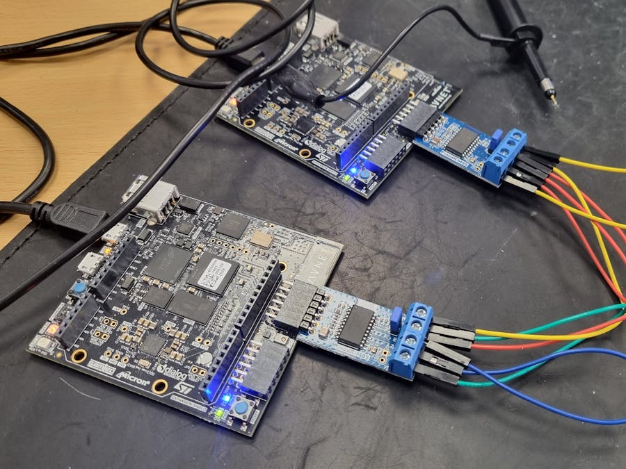
There are many application level protocols which can be implemented using these physical layers. In this project we are going to look at connecting together two MiniZeds using RS485 Pmods and a bespoke application layer protocol.
Application layerThe custom communication protocol implemented is going to enable the master MiniZed to be able to read or write a 32 bit word from a 16 bit address space within the slave MiniZed. For this project we will be reading and writing from a BRAM in the slave. However, this BRAM could be being populated by the sensors gathering data on the slave MiniZed.
Data will be sent over the RS485 link using a UART with a packet containing several UART transmissions
The format of the write is
<STX><ADDR MSB><ADDR LSB><Data MSB><Data><Data><Data LSB>
The slave will respond to a write with a single byte ACK or NACK
The format of an read is
<ENQ><ADDR MSB><ADDR LSB>
The read response from the MiniZed slave will be
<SOH><ADDR MSB><ADDR LSB><Data MSB><Data><Data><Data LSB>
The SOH, STX, ENQ, ACK and NACK are defined in the ASCII table
Of course this protocol could be implemented using a UART in a processor like the ZYNQ however, to make the protocol scalable. I have created custom RTL modules for the UART, Protocol Master and Protocol Slave.
As the RS485 is directional on the same twisted pair the protocol must only enable the RS485 transmitter when it ready to transmit to reduce the potential for contention on the bus when multiple transmitters attempt to transmit at the same time.
MiniZed Master.The MiniZed Master design will use the PS core to send and receive data over the RS485 Interface. This will enable the link to be tested as data should be able to be written across the link and then read back in different order from the Block RAM in the MiniZed slave.
The design uses AXI GPIO modules connected to the Protocol Master module to drive the Interface requirements of the protocol master block. This includes the Address, Data and read or write action. The result provides the address read from and the read data.
To be able to debug the application I included several ILA's as well, help understand the system behavior.
The software application running on the Minized Master is
#include <stdio.h>
#include "platform.h"
#include "xil_printf.h"
#include "xgpio.h"

#define DATA_ADDR  XPAR_GPIO_0_DEVICE_ID
#define VALID_RW   XPAR_GPIO_1_DEVICE_ID
#define DATA_BCK   XPAR_GPIO_2_DEVICE_ID
#define DATA_VALID_CH 1
#define ADDR_RW_CH 2

XGpio Gpio1;
XGpio Gpio2;
XGpio Gpio3;

int count = 0;

int main()
{
    init_platform();

    XGpio_Initialize(&Gpio1, DATA_ADDR);
    XGpio_Initialize(&Gpio2, VALID_RW);
    XGpio_Initialize(&Gpio3, VALID_RW);

    while(1){

    u32 rd_data, rd_addr;
    //write

    XGpio_DiscreteWrite(&Gpio1, DATA_VALID_CH, count );
    XGpio_DiscreteWrite(&Gpio1, ADDR_RW_CH, 0x5001);
    XGpio_DiscreteWrite(&Gpio2, ADDR_RW_CH, 0x0);
    XGpio_DiscreteWrite(&Gpio2, DATA_VALID_CH, 0x1);
    XGpio_DiscreteWrite(&Gpio2, DATA_VALID_CH, 0x0);

    usleep(1000);
    //read
    XGpio_DiscreteWrite(&Gpio1, ADDR_RW_CH, 0x5001);
    XGpio_DiscreteWrite(&Gpio2, ADDR_RW_CH, 0x1);
    XGpio_DiscreteWrite(&Gpio2, DATA_VALID_CH, 0x1);
    XGpio_DiscreteWrite(&Gpio2, DATA_VALID_CH, 0x0);
    usleep(10000);

    rd_data = XGpio_GetDataDirection(&Gpio3, 1);

    rd_data = XGpio_DiscreteRead(&Gpio3, 1);
    rd_addr = XGpio_DiscreteRead(&Gpio3, 2);

    if(rd_data != count){
    	printf("read back not correct %d, %d \n\r", rd_data, count);
    }

    usleep(1000000);
    count++;

    }
    cleanup_platform();
    return 0;
}The MiniZed Slave uses the PS module to provide the clocks for the logic design. The Protocol Slave is connected a BRAM which stores the data provided over the communication link.
There is no software needed in this implementation of the MiniZed Slave just the Protocol Slave, UART and BRAM. As with the MiniZed Master the PS provides the clocks for the modules.
Common XDCBoth the MiniZed Master and Slave use Pmod 1 on the MiniZed to connect to the RS485 Pmod. As such the XDC files for both are the same.
set_property IOSTANDARD LVCMOS33 [get_ports {re[0]}]
set_property IOSTANDARD LVCMOS33 [get_ports de]
set_property IOSTANDARD LVCMOS33 [get_ports rx]
set_property IOSTANDARD LVCMOS33 [get_ports tx]
set_property PACKAGE_PIN L15 [get_ports {re[0]}]
set_property PACKAGE_PIN M14 [get_ports de]
set_property PACKAGE_PIN L14 [get_ports rx]
set_property PACKAGE_PIN M15 [get_ports tx]The RS484 bus is pretty straight forward but we do need to wire up the Pmods properly as shown in the Digilent PmodRS485 reference guide.
The two ends of the RS485 terminal need to be terminated with a resistor, on the PmodRS485 this can be fitted or not using a jumper. For this application both resistors need to be fitted.
When wiring this up be careful to connect the loop back for the receiver on the Pmod.
Testing In HardwareUsing the software application running on the MiniZed master we can read and write the BRAM memory in the MiniZed slave. However, to understand how it works we learn best from looking at the waveforms on the bus
The transmission for a write from a master on the logic TX pin looks like below
The corresponding bus side looks as below - note the 0x06 at the end is the acknowledge.
The RX pin on the logic RX signal at the master shows the write and the write acknowledge. The designs on both the MiniZed Master and Slave have the RX permanently enabled
Reading from the MiniZed Slave looks as below, with the data representing a incrementing count written in by the MiniZed Master.
In the waveform below the read request can be observed on the bus side, prior to the read response.
The timing of the TX Enable with respect to the TX Data is shown below note how we disable the TX path when a reply is expected.
Probing the different TX enables on the MiniZed Master and Slaves shows how the
FPGA make great solutions for many industrial applications, this project has demonstrated how easy it is connect different boards and transfer data using commonly used industrial interfaces. In this application the data rate was 1Mb/s put line rates up to 16Mb/s or faster can be achieved!


Comments