


Hardware components | ||||||
 |
| × | 1 | |||
 |
| × | 1 | |||
Software apps and online services | ||||||
_4YUDWziWQ8.png?auto=compress%2Cformat&w=48&h=48&fit=fill&bg=ffffff) |
| |||||
| ||||||
This project is going to be slightly different compared to previous projects. In those projects I have implemented FPGA / SoC designs which run on existing boards.
However, in this project we are going to go through the steps required to make our own custom board which can be used with the Ultra96. This board will perform the following
- Break out the low speed connector to two PMOD interfaces.
- Break out the high speed connector to a SYZYGY interface.
This board will therefore enable me connect a range of PMODs and SYZYGY pods to the Ultra96.
My plan is to design the board in the project, get it manufactured and then follow up with a project showing it working.
To get started with this we first need to define the architecture of the board itself, but first we need to define the tool chain we will be using.
Tool ChainTo keep the open tool chain as much as possible, I will be using open source tools for schematic capture and layout. Therefore I installed KiCad which will allow me to design the schematics, perform the layout and even visualize it in 3D.
Another bonus for choosing this tool is 96 boards provide a KiCad template for consumer edition boards which makes the layout easier.
We can also use this KiCad library for implementing the Pmod connections.
StandardsAs we are going to be interfacing with the Pmod and SYZYGY standards we need to be able to ensure we are complaint with them. The standards can be found online at
It is these standards we will use to make sure we interface properly, although we face a slight challenge, in the SYZYGY interface which we will address later.
ArchitectureIn the architecture of the design we are going to determine how we can connect the HS and LS connectors to the PMOD and SYZYGY connectors. Along with the basic connectivity we will be looking at the power supplies needed along with additional signals.
First the Pmod interface, I want to be able to use the existing Digilent Pmod IP cores. These cores us the PL therefore the PL connections from the LS connector are what we will be using to connect to the Pmod breakouts.
Luckily there are 16 GPIO which are connected to the PL bank 26 which has a 1v8 VIO
The HS connector provides a 12 differential pairs designed for MIPI connected to banks 66 and 65 which operate from a 1v2 VIO.
Power wise the LS connector provides Vin (12v), 5V and 1V8, this means on the mezzanine board we need to generate a 3v3 and 1v2 rail.
We need 3v3 for the Pmod, which also means we need to level translate the signals. We also need 1v2 for the VIO of the SYZYGY, as the differential signals will be using this standard and we do not have a 1v2 rail available.
We can do this as the return on the Mezzanine is the same as return on the Ultra96
To create the 3v3 we will use a Dc Dc convertor which steps down from 5V to 3v3, as this could potentially require significant currents a switching converter is used to minimize losses.
For the 1v2 rail we will also use a buck converter to step down from 5V, this will ensure the VIO current max of 2A can be supplied.
We also need to be able to translate levels between the Pmod and LS connector, this can be a challenge as different Pmods use different IO standards e.g. SPI, I2C and UART which changes pin directions.
As such to make sure support is available for maximum flexibility we need to use automatic bi directional level shifters to convert between 1v8 and 3v3.
The completed architecture of the design looks like below, to ensure the Ultra96 can be powered on and off as well the mezzanine board will also include the power and reset buttons.
To determine the pin out between the HS, LS, Pmod and SYZYGY connectors I created two simple tables. to show the mapping.
On the HS to SYZYGY connector break out the pins highest pins are not connected to the MPSoC but to the USB
Now we are ready to create the schematics, we can do this by in KiCad selecting new project from template and selecting the 96 boards template we installed earlier.
This will provide the template selector and we can select the 96 boards mezzanine template. This only contains the low speed connector but we will get the the high speed connector later.
Once we are ready with the template we can open the schematics and capture the design. If you need to find new symbols for components which are not in the kiCad library I used the samacsys which generates symbols, footprints and 3d images for the component along with automatically installing to KiCad.
The completed schematics can be seen below
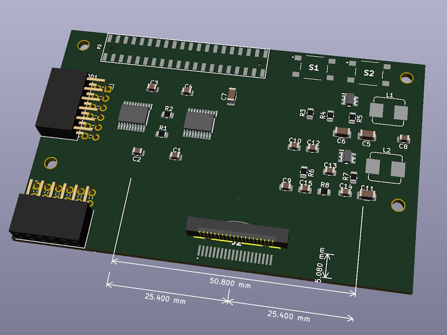
Once the schematics are completed the next stage is to pull the components through to the PCB and place the components.
LayoutOf course we can use both sides of the board however, on this design I only want to have the high speed and low speed connectors on the bottom of the board.
All the remaining components will be placed on the top of the board. Critical elements of this placement are the high speed connector location which must comply with Avnet Mechanical Drawing, we must also comply with the SYGYZY keep out areas around its connector.
Once these components have been placed, we can view what the PCB will look like once manufactured using the 3D viewer.
All that remains now is the routing of the board, this will be implemented on a four layer PCB so we have better impedance control.
The SYGYZY signals need to be capable of running at up to 500 MHz, as such the layout and signal integrity is critical. I have there asked a friend of mine who does PCB layout to layout the board. Once I get the file back I will share them on my github for people to access and use as desired.
I will also be having several of these made for testing and use in my own projects going forward.
Wrap UpCreating the architecture, design and placement of the breakout board has been very interesting and different to my previous projects.
I really cannot wait to get one in my hands and start bringing it up and creating projects based on it!


_Ujn5WoVOOu.png?auto=compress%2Cformat&w=40&h=40&fit=fillmax&bg=fff&dpr=2)


Comments
Please log in or sign up to comment.