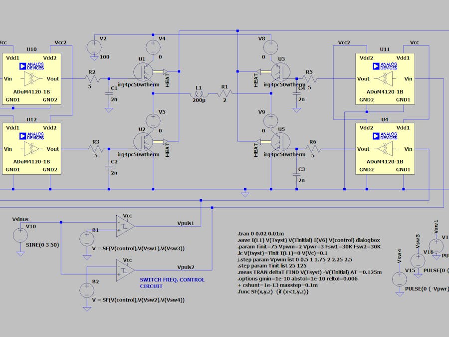
Warning: the following simulation intends only to show how a full IGBT bridge can be simulated with gate drivers and taking account of thermal effects. It is thus intended for educational example only without assurance on practical results. The primary goal is to show that when proper models are available, very realistic results of a relatively complex schematic can be obtained within a short time. The strategy exposed for the derating in temperature works on "paper" but has not been tested in the practice and intends only to develop engineer's intuition.
The used models belong to their respective owners (Analog Devices for the gate drivers, for the Infineon IGBT, consult the netlist provided in appendix, and the thermistor is a Vishay model).
Like most simulations, the results are a bit self explanatory. The gates are pulsed with a signal resulting from the comparison of a 50Hz signal compared to a 30 KHz sawtooth signal. This PWM is better seen a a lower frequency as presented in the following screen (3 KHz).
At 30 Khz, the modulation is high enough to produce a nearly 50 Hz sinusoidal current into the load.
The IGBT models have been replaced by the thermal models whch show a supplementary pin, which is the pure heat amount source produced by the devices. The thermal pins of the IGBT's are all connected together to the heat sink and to a voltage source which is the ambient temperature.
At high temperature, the duty period is reduced : the IGBT switching is derated, which induces less heat into the heat sink and the temperature stabilizes. More information over the sumulation can be obtained at edesign.ntc@vishay.com


Comments
Please log in or sign up to comment.