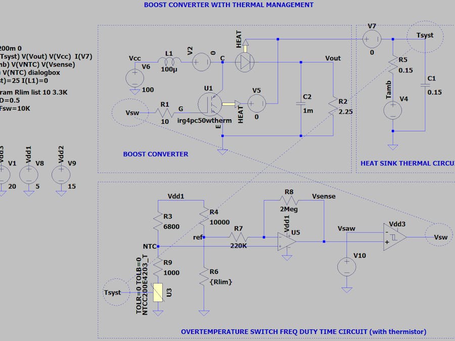
This boost converter simulation shows a possible derating of voltage ratio Vout/Vin when temperature rises up above a certain threshold. The duty cycle begins then to decrease (by the pulse wave modulation applied to the gate of the IGBT). The temperature is measured by a Vishay NTC (Wire bondable die NTCC200). The IGBT and diode models have been transformed into thermal models (a supplementary output pin models the internal heat created into the devices ; this pin is directly connected to the thermal RC network modeling the heat sink). The final temperature Tsyst is measured by the NTC, including into a small circuit which produces a PWM of the gate of the IGBT.
This first capture gives a circuit topology of the Boost converter, with the thermal circuit.
This second capture represents the Vin and Vout variation (above pane), the Vsense (mid pane) and on the lower pane the system temperature and the ambient temperature. When the temperature limitation is activated, the system temperature Tsyst stabilizes just a few degrees above an ambient temperature of 100°C, as the ratio Vout/Vin is reduced to 1 (full derating).


Comments