Power Bank for Smartphones
(This project is being managed here: Project Repository )
Background StoryThe use of mobile phones is increasing day by day due to the involvement of digital and online things in our lives. During the period of the pandemic, when offices and educational institutions were closed due to the risk of spreading Corona, everyone shifted their work to the online mode. In the online working, a large backup of battery is required to continue the work. Students and workers have to face the problem of insufficient battery in mobile phones when they do not have the access to electricity or an ordinary charger. The power bank gives them the facility of charging their mobile phones at any time especially when they do not have the charger. The users just need to charge their power bank at once and then they can charge their mobile phones without any interruption.
Creating a power bank on PCB is very simple but the task to send it to the manufacturer for fabrication is quite difficult for me. I avoid going to the manufacturer, so I have created my project online on Inventhub. Through Inventhub I can get connected to the manufacturer and component provider directly. This online platform gives me the facility of creating the Bill of Material (BOM) of my project that helps me to send my components list used in the project with exact parameters including value, footprint, and manufacturer.
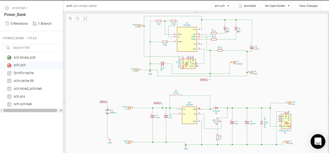
WorkingIn this project, I have used TP4056 that is used to provide constant liner voltage to the battery in the power bank. There are two parts in this circuit one is the charging circuit and the other one is acting as a boost converter to boost the voltages from 3.7V to 6V. In the first part of the circuit, I have used resistors of 1kohm to balance the provided voltages then two LEDs to show the indication of charging and a micro USB port to plug in my charging device.
The other part of the circuit consists of a boost converter that is XL6009 to boost the voltages and a potentiometer of 5kohm to send those voltages as an output. Micros USB port is attached at the output end to charge the mobile phone.
Schematic DiagramI have created this schematic on KiCAD. KiCAD is very simple and easy to design your PCB. By going into the new project click on Schematic and then you can create a new schematic diagram for your project.
In the schematic diagram, you can see that circuit is divided into two parts. The upper one is the charging circuit that will provide constant voltages to charge a device. The lower one is the boost circuit that will boost the voltages and will help in charging your mobile phone.
I have created it online on Inventhub so that I can get connected to the manufacturer, suppliers, and engineers. I can show my project to them and then they can send me the revisions I need to make in my schematic to improve my project.
Here is the link where you can find my project.
https://inventhub.io/c/arshmah/Power_Bank/tree/default
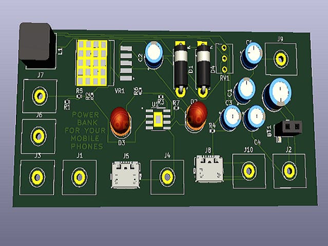
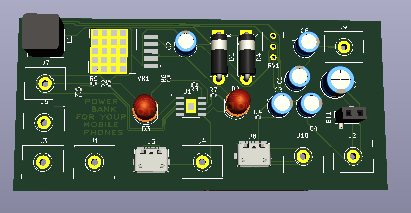
Online PCBAfter creating the schematic diagram I converted my schematic file to the PCB file where I can see my design onboard and can arrange the components onboard according to my own choice of making my board of the compact size that is preferable in designing.
Below is the link where you can find my project online.
https://inventhub.io/c/arshmah/Power_Bank/tree/default
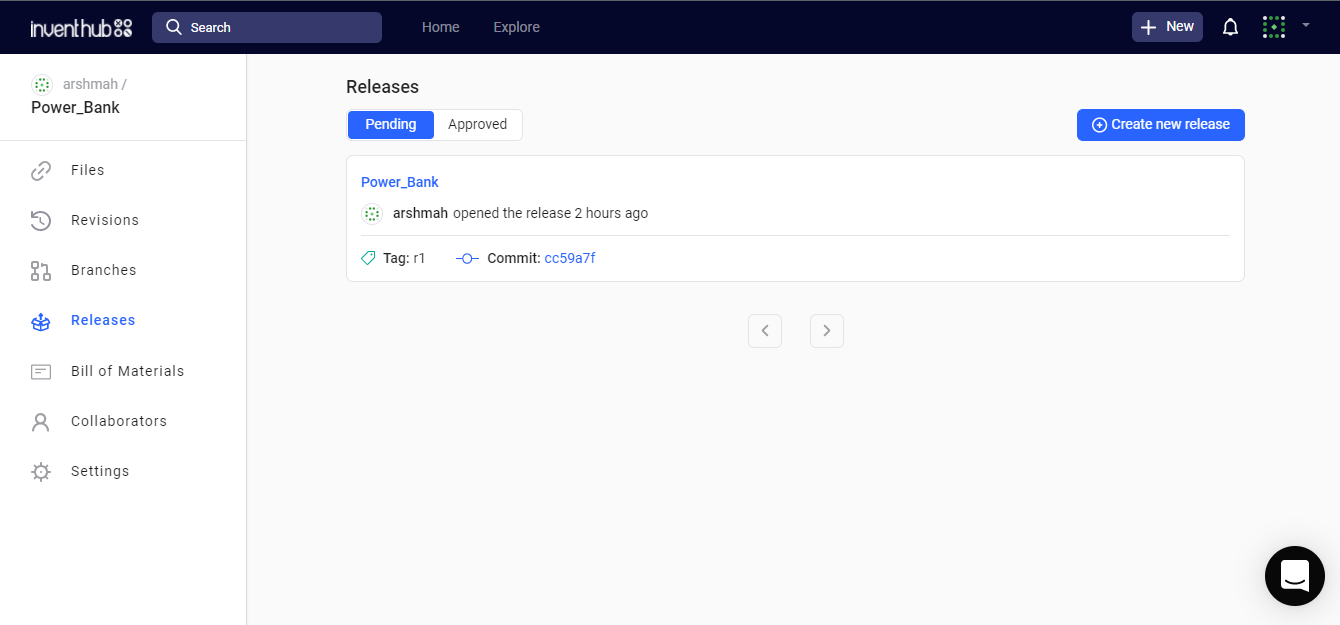
Design For ManufacturingOnce I have done with the schematic and PCB design on KiCAD the next step would be to send it to the manufacturer to fabricate it. For fabrication, I need to provide the manufacturer with all project files including routing layers, footprints, component and board size, etc. For this, I have created the release of my project that will allow me to send my whole project files to the manufacturer directly without any error.
I have created the online release of my project on Inventhub. Where the manufacturer can find all my project files in a zip folder he just needs to download it to start I do not need to visit him manually to fabricate my PCB I can get it online easily.
This is the link to the online release of my project.
https://inventhub.io/c/arshmah/Power_Bank/release/r1
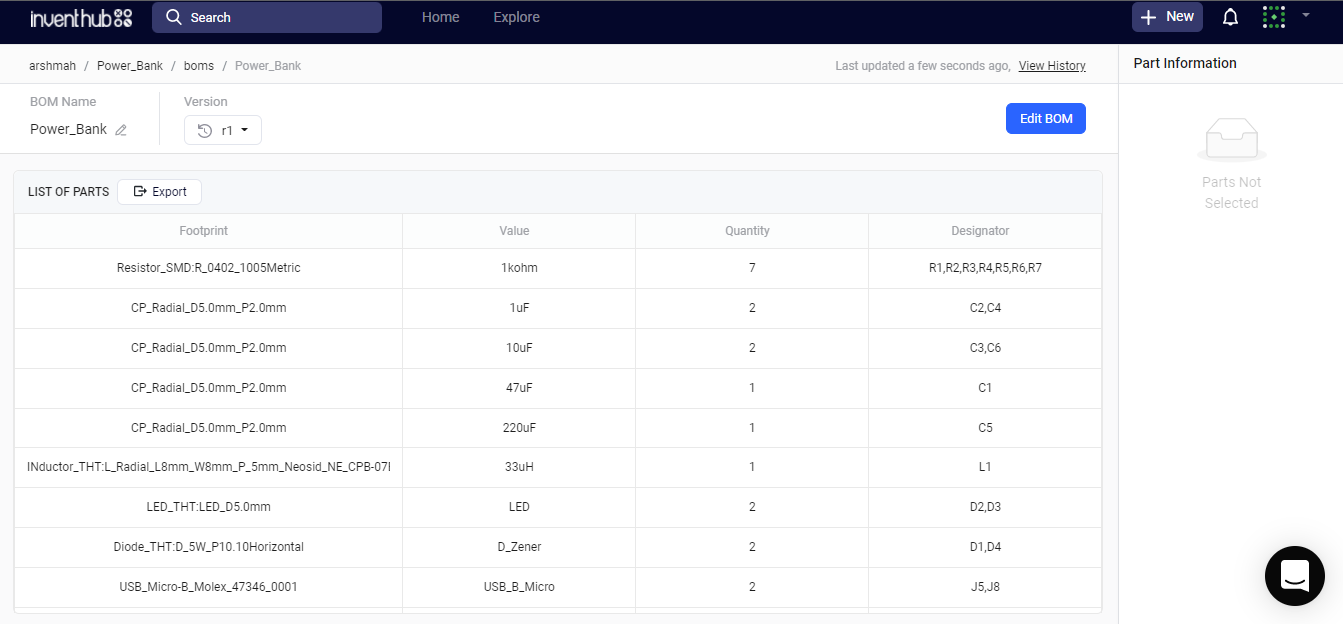
Bill of Material (BOM)After the fabrication of PCB here comes the next step to attach the components to the board. For this, I need to get connected to my component provider to provide me with components of the exact parameters I need. I have created a BOM i.e. a list of components with the same dimensions and footprints on Inventhub. I do not need to create an excel file to write the list of components, I have just created the BOM where the component provider can get the file he just needs to export the file in CSV format and he can send me the same component I need.
Here you can find the complete BOM of my project.
https://inventhub.io/c/arshmah/Power_Bank/bom/list
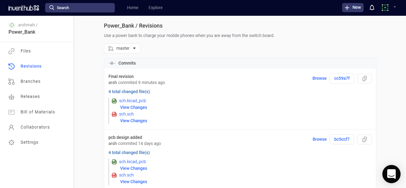
Revisions in the ProjectRevisions in the project allow users to improve the project. I have created the revisions in my project on Inventhub. If I have made any mistake in designing then the collaborators working with me can mention my error and I can make it correct and upload it again with the new change.
If you have any questions feel free to reach out.






Comments
Please log in or sign up to comment.