(This project is being managed here: Project Repository)
Motivation behind the projectNowadays students have become smart enough that they can bring their mobile phones to the exams hall where they are strictly not allowed to use mobiles. Sometimes teachers can find phones but when there is a large number of students it is hard to check every student manually. This mobile phone detector can easily detect any RF transmitting device. This is portable, easy to carry, and accurate in detecting the presence of mobile phones.
Working on the projectThe MOSFET OP amplifier CA3130 used in this project is used to detect mobile phones in restricted areas. Whenever there is a mobile phone detected in an area it will go high and will lighten up the LED showing that there is a phone otherwise it will remain off when there is no phone detected. The capacitor 0.22uF attached with the OP amplifier will act as an RF signal detector which will further send the signal to the OP amp that will decide whether there is a phone or not. It is a frequency detector circuit that will detect the frequency of a defined range and will convert that signal to some voltage or current level like in the form of LED to tell the presence of any device.
A mobile phone detector with all the components can be arranged in the following pattern to make a phone detector to avoid the entry of mobile phones in restricted areas.
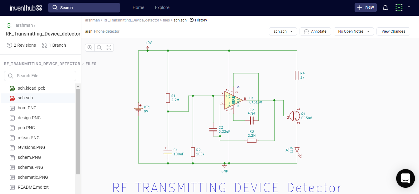
BY creating a new schematic file I have designed this diagram, in the diagram we have a battery to provide the supply to the circuit then we have a capacitor and resistor to make a path for the MOSFET to detect the presence of a mobile phone. We also have an LED at the load side to show the presence or absence of mobile phones in exam halls.
After creating the design on KiCAD I have shifted my project to the online platform Inventhub where I can show my design to my manufacturer and can send it to him for fabrication.
This is the link where you can find the schematic diagram of the project https://inventhub.io/c/arshmah/RF_Transmitting_Device_detector/tree/default
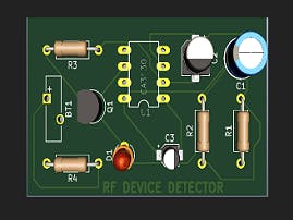
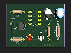
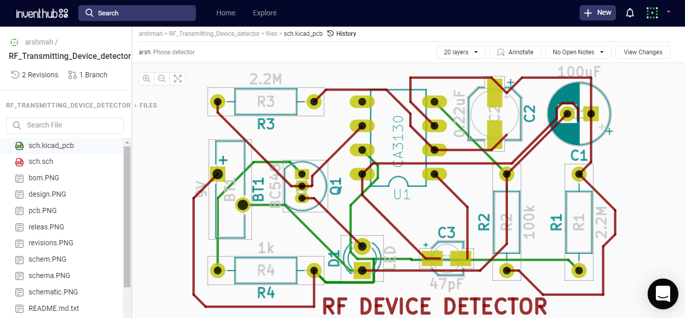
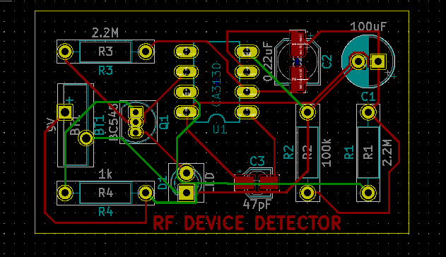
PCB designPCB design is necessary to get the final design of the project. After creating the schematic I have converted the schematic file to the PCB design file. Where I have selected the arrangements of the components so that I can route each component without overlapping the routing track otherwise it gives me an error. Then I draw the size of the board according to the size and arrangements of the component. After implementing routing on the design I checked if is there any error, using the Design Check Rule. I tried to make it a compact size so that I can achieve a goal to keep it in my pocket. In the last, I clicked on the option of 3D view to view its PCB board view.
I will then take my final design to the online platform Inventhub to get my final hardware-designed PCB from the manufacturer.
This is the link where my PCB file is available https://inventhub.io/c/arshmah/RF_Transmitting_Device_detector/tree/default .
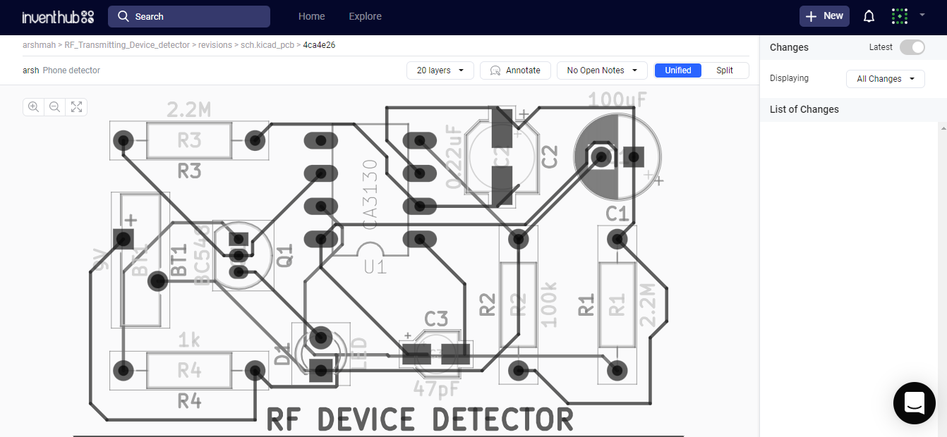
Revisions of the projectThe purpose of creating revisions is to keep the updated file at the topmost. If there is an error in my design I will change it and will upload the revised edition of my project.
In Inventhub I have created revisions that is mean if my collaborators are giving some suggestions to add or remove something in my project I can make them and can upload their latest revision. This feature allows us to view our older and newer versions of the project.
Here is the link where you can see the revisions in my project https://inventhub.io/c/arshmah/RF_Transmitting_Device_detector/commits/default
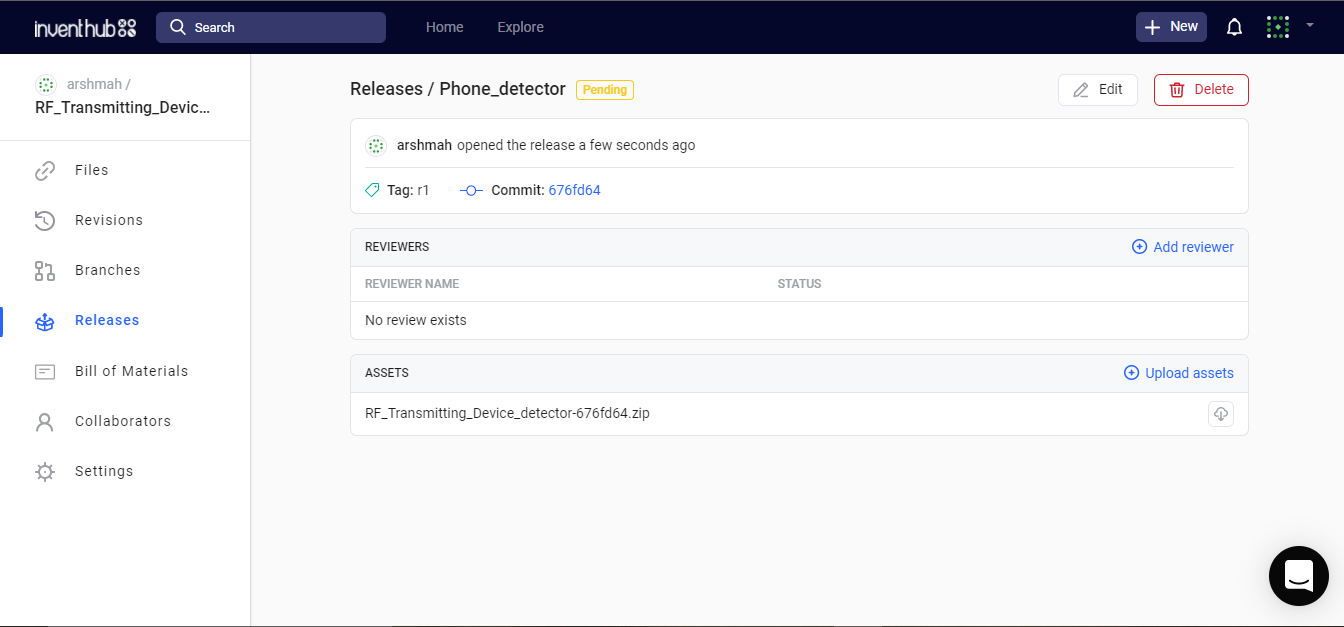
Design for ManufacturingAfter creating the schematic and PCB designs I can send them to the manufacturer for fabrication. For this, I have to send them my all project files so that he can fabricate the PCB accurately without missing any part in it. I will release the project that will allow me to make a zip file of my RF transmitting device and the manufacturer simply export it to fabricate. This can be done by using Inventhub, I have created a release of my project as a zip file where I can download that file without any error or changes.
Here is the link to find therelease of my project https://inventhub.io/c/arshmah/RF_Transmitting_Device_detector/releases/pending
BOM(Bill of Material)After getting the fabricated PCB in the hard form from the manufacturer then you need to solder components on the PCB.
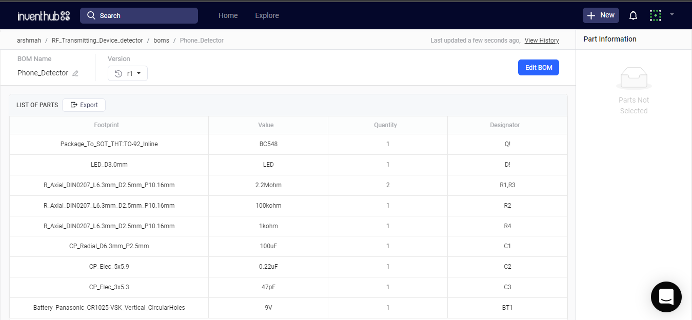
At the final stage of my design, I need components for my project. I can create a Bill of Material on Inventhub with all types of footprints with names of the component and I can get my components from the service provider. Below is the link to my complete bill of materials for this transmitting device detector.
https://inventhub.io/c/arshmah/RF_Transmitting_Device_detector/bom/list






Comments
Please log in or sign up to comment.