Industry 4.0 is about smart equipment communicating with each other. Also equipment will have self maintaining capabilities, by collecting data about their condition and letting an AI to predict malfunction.
A wireless switch (kind of a wireless solid state relay) with smart functions like current measuring, will ease the creation of smart equipment. It should be easy to integrate in existing equipment and by measuring the current consumption of the device, using AI and big data analysis malfunction could detect with high precision.
In terms of design requirements and features we have something like:
- voltage range: 12-300 VDC, 87-230 VAC
- current range: 0-50 A (DC / AC)
- high efficiency - low ON state resistance (comparable to a mechanical relay)
- high reliability - no moving parts
- (truly) wireless operation - the only connections are the power and load
- built-in modular power supply - 12V (modular) for gate drive and 3.3V for logic
- safety - automatic malfunction detection (over-current), automatic turn-off in case of connection / HB loss
- speed / power control (PWM)
- security - secure communication and firmware upgrades
- compact size
The Infineon’s 600 V CoolMOS™ C7 Gold MOSFET-s can be used to build such switches. Given its low Rds enables high efficiency, while its robustness (600 breakdown voltage, improved body diode) enables way much higher reliability than a mechanical relay based could offer. The low PCB footprint and thermal properties enables compact design (50x70x25mm).
On the software side the device exposes a HTTP interface and it also publishes its state and sensor data over MQTT. The HTTP interface is secured using modern cryptography. The data broadcast-ed by the device is saved in time-series databases, to be used later for data visualization & analysis, AI and so.
Here is how the concept image of the CoolSWITCH device looks like:
And this is the finished PoC device:
Power supplies and different variants of the main board:
Demo Video, showing the most important features of the CoolSWITCH:
AC / DC SwitchIn order to create a switch that can handle both AC and DC loads two MOSFET-s are needed.
To switch a DC load a single is MOSFET (Q1) is enough. The source is connected to the DC ground (DC-), while the load is placed between the drain of the transistor and the positive terminal of the DC power supply (DC+).
When a positive voltage Vgs, higher than the gate threshold voltage Vth is applied to the gate the MOSFET will start conducting and the switch will be in the ON state. In OFF state, when Vgs = 0V the MOSFET will block the current.
However, in an AC setup with a single MOSFET only the positive half cycle of the AC signal can be controlled. In the negative half cycle the current would get passed by the body diode of the MOSFET, regardless of the gate voltage.
To solve this problem, two MOSFET-s (Q1 and Q2) with opposite orientation (common source) can be connected in series. In this configuration, each MOSFET controls one of the half cycles of the AC signal, while always conducts in the other half cycle. The gate and source pins of the MOSFET-s are connected together, so this setup will function as the above DC signals. When Vgs > Vth the switch will be in ON state, while if Vgs = 0 the switch will be in OFF state.
For a DC load the second MOSFET (Q2) is optional. When Q2 is present, the two MOSFETS can be used in parallel (by connecting the drains of the MOSFETS. This will allow bigger loads and can also prevent overheating.
Gate DriveTo turn on the MOSFET a voltage higher than the gate threshold voltage Vth of the transistor is needed. In the case of the CoolMOS, the Vth is 4V (max). However for higher efficiency, a higher gate voltage > 10V is recommended.
To drive the MOSFET-s a dedicated gate driver IC can be used. It is recommended to use one with electrical insulation.
The Infineon EiceDRIVER™ 1EDI series provides this in a compact package. The chip is divided in two galvanic insulated parts.
The input side takes a supply 3.1- 17V and pair of input signals (IN+/-). The output takes a supply 10-35V and generates the OUT+ and OUT- signals to drive the gate.
To drive the MOSFET-s the following setup can be used:
On the input side 3.3V logic signals are used. The IN- is ties to GND (logic), while the IN+ will control the state of the switch: 3.3V = ON, 0V = OFF.
The output side takes a supply of 12V. The OUT+ and OUT- are connected to the gate of the MOSFETS through the R3 and R1 resistors. The R3 is used to set the gate charge current, while R1 to set the gate discharge current.
Wireless LogicThe micro-controller used in this project will be the ESP8266. The ESP8266 is a 32-bit RISC micro-controller with built in 2.4 GHz WiFi and TCP/IP stacks.
It comes in a number of ready to use modules. In this project I will use the ESP-12-E module:
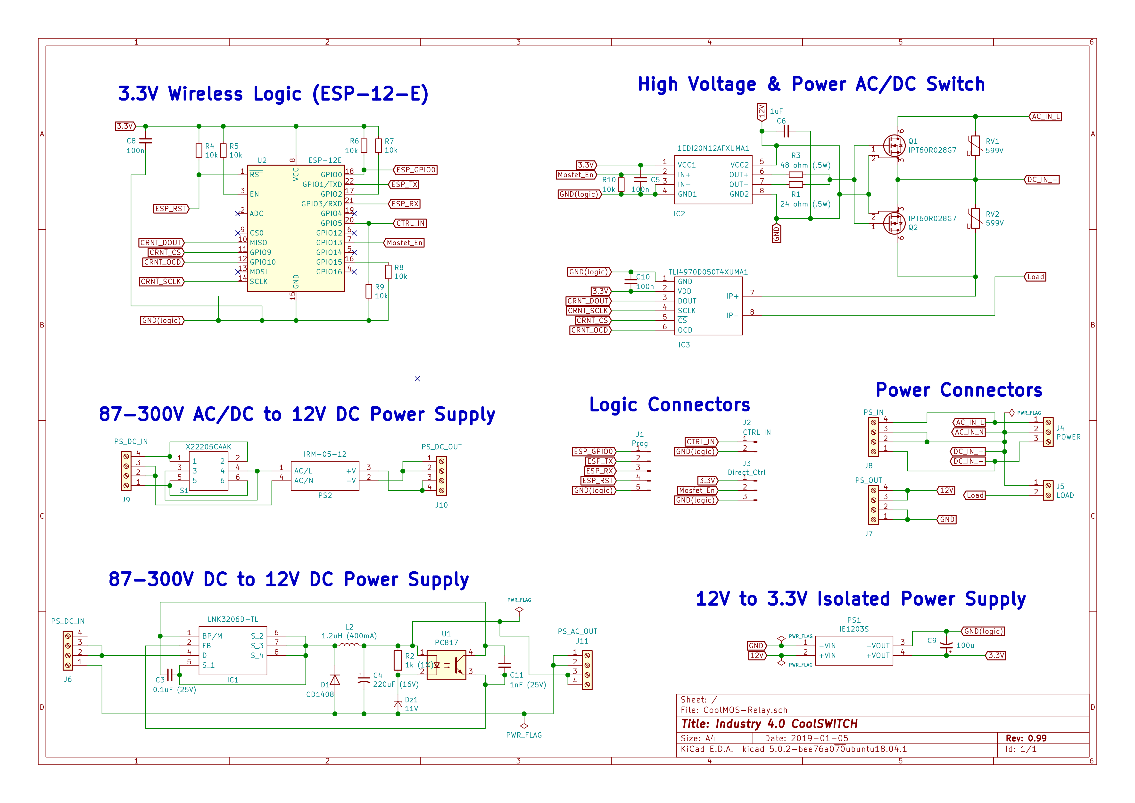
The ESP-12-E module is connected in the circuit as follows:
I also added a some pin headers for direct control and programming:
For industry equipment reliability is very important and sensor data from the equipment can help detecting malfunctions early.
Our wireless switch will include a current sensor to continuously measure how much current the load consumes. A sensor the provides this functionality is the Infineon TLI 4970 current sensor.
The TLI 4970 runs if high precision current sensor that runs on 3.3V, provides data over an SPI interface has galvanic insulation between the power and logic sides. This means it can be very easily connected with the ESP-12-E module.
The current data will broadcast information to a central database. Then AI can be used to detect anomalies. In case of excessive current the equipment can be turned off automatically.
The sensor is connected in parallel with the load as follows:
The project will include power supplies to generate from the power lines the voltages needed by the gate drive and wireless logic circuits.
As we have seen, the project needs two voltages:
- 12V - used in the power side to drive the gate drive - as it is referenced back to the power lines (through the MOSFET's source), it can be either insulated or non-insulated
- 3.3V - used for in the logic side - must be insulated from the power side
The 12V will be generated by modular power supplies. This is needed as the switch will be a able to operate in a wide range of input voltages (15-300V DC, 87-230 VAC). Each module will work in a a specific AC or/and DC voltage range. We will see the module designs later.
The 3.3V supply will be generated from the 12V using a XP Power IE1203S insulated power supply module:
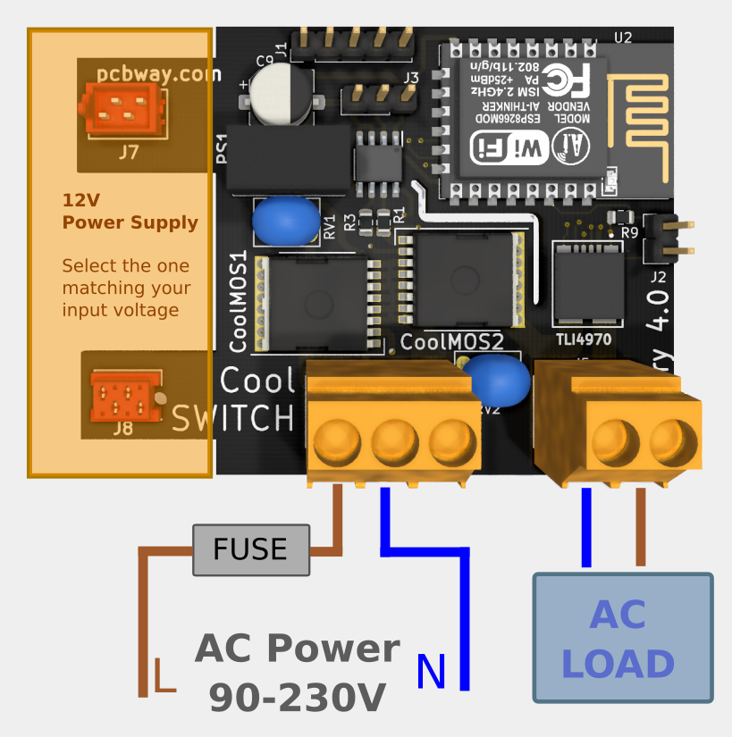
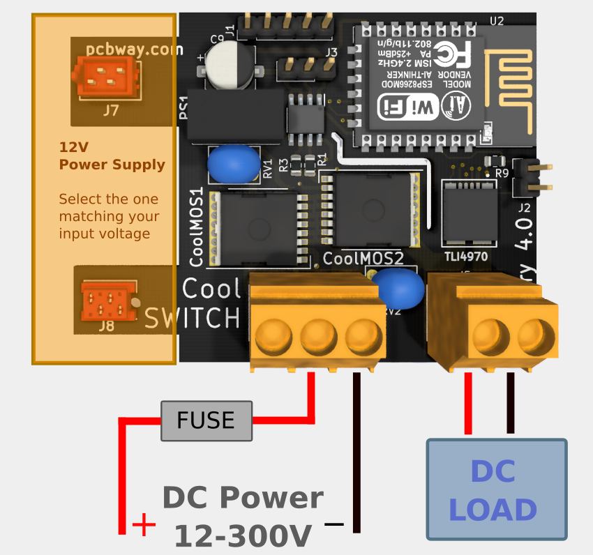
The AC or DC power will be provided through a 3 port screw terminal (J4) as follows:
The J7 and J8 board to board connectors will be used to attach the appropiate 12V power supply module.
The load will be connected to a 2 port screw terminal (J5).
The RV1 and RV2 are 599V TVS varistors used to protect the MOSFET against voltage surges over 600V.
PCB DesignThe schematics and the PCB was drawn in KiCad open source electronics design automation suite:
The PCB was designed to be as compact as can. The result is a approx. 70x50mm board with 3 zones:
- power zone - high voltage / power switching, gate drive, current measurement
- logic zone - for 3.3V logic, isolated from the power zone
- 12V supply - the place reserved for modular 12V supplies (the 12V supplies are connected using Micro-MaTch series board-to-board connectors, rated @ 230AC)
The components on the PCB are arranged as follows:
In terms of clearances and creepage the power zone uses 2 mm clearance.
The PCB are manufactured by pcbway.com. 2oz copper layer to handle high current and black silkscreen for nice look. pcbway.com offered to sponsor the PCB-s for this project, so I just had to pay for the shipping.
This is how the PCB-s look like:
Given the high range of input voltages and types, the 12V for the gate drive circuit is generated by modular power supplies. The modular power supplies connects to the main board using MicoMatch series 1.27 mm pitch 230 VAC rated board-to-board connectors.
These are the following 12V power supply variants:
100-230 VAC / VDC Isolated Power Supply Module
It is based on the on the IRM-05-12 module, which is an all in one power supply module with 100-220 VAC / DC input and 12V output
On the bottom of the module there is a switch to select between AC and DC input.
87-300 VDC input non-isolated power supply
(work in progress)
Custom design based on the LNK3206 IC. It is non-isolated, but this is not a problem as we will reference the GND back to power rail anyway, through the source pin of the MOSFETS.
The design is a simple buck converter circuit topology with the LNK3206 doing the switching, while the feedback circuit is based on a 11V zener and an opto-coupler.
15-80 VDC input non-isolated power supply
(work in progress)
Power supply for low voltage DC application. An Ebay power supply module will be used to implement this.
12V-12V dummy power supply module
Main board PCB and components in pieces
and assembled:
100-230 VAC power supply module in pieces
and assembled:
100-230 VAC power supply module in pieces:
and assembled:
Except the MOSFET-s, I got the rest of the components and the PCB and prepared some test code, so we was ready for a smoke test.
Also, I assembled the main board and did some tests. For the first test, the classic Blink, I used the programming port of the board, a breadboard and a Serial to USB converter:
This worked, so I uploaded a Sketch which uses WiFi. Also enabled the standard Arduino OTA upload functionality on the ESP-12E, so the firmware can be updated wirelessly.
I tested the 12V-3.3V power supply with a 12V-12V power supply module:
To test the TLI4970, I used a 47 Ω resistor and applied different voltages to it:
The current values measured by the TLI4970 looks like this:
Mains (230V) power supply test:
This week, I purchased two CoolMOS C7 (IPT60R028G7XTMA1) MOSFET-s, so finally I was able to make some switching tests.
First, I did some tests on 12 VDC:
Then, on 230 VAC:
Both worked fine.
SoftwareThe code of the CoolSWITCH runs on the ESP-12E and it was written using Arduino (C++).
It is divided in multiple components (C++ classes). Each components has a .begin() and a .handle() method. These are called from the setup() and loop() methods of the Arduino Sketch.
CoolSwitch is the most important component. Contains the state machine controlling controls the two MOSFET-s of the switch, based on the sensor data and HTTP interface inputs. The states of the state machine are: 0 - OFF, 1 - ON, 2 - SOFT_START, 3 - SOFT_STOP, 4 - OVER_CURRENT.
CoolSwitchConfig contains code to save and load properties (such as Wifi settings) from the ESP-12E's flash memory. The properties are saved as files on a SPIFFS file system.
CoolSwitchCurrentSensor handles the communication with the TLI4970 current sensor. Under the hood uses the TLI4970 library from Infineon.
CoolSwitchHTTP contains the implementation of the HTTP / REST interface. It exposes the following endpoints:
/- root endpoint, returns a hello message with the device's name/turnOn- turn the switch ON/turnOff- turn the switch OFF/setValue?prop1=value1&...- set the value of different properties / settings. The available properties are wifiSSID (String), wifiPassword (String), mqttServer (String), mqttPort (int), speed (float %), currentLimit (float Amps), softStartStop (true|false), softSwitchDuration (milliseconds)/state- returns the current state of the switch (0 - OFF, 1 - ON, 2 - SOFT_START, 3 - SOFT_STOP, 4 - OVER_CURRENT)/current- return the current consumption measured by the TLI4970/secret- can be used to perform a Diffie-Hellman key exchange, in order to secure the HTTP and Arduino OTA interfaces/reboot- reboot the ESP-12E/factoryReset- clears the setting saved in the flash memory and reboots the device
CoolSwitchMQTT is responsible for publishing data over the MQTT protocol. Currently, two data feeds are published:
CoolSWITCH-XXXXXXX/state- the current state of the switchCoolSWITCH-XXXXXXX/current- the current consumption measured by the TLI4970
I also wrote a small Pyhton client (HTTP) for the CoolSWITCH. This along with the rest of the source code can be found in the in the GitHub repository,
First Start - Device name, Wifi & NetworkingEach CoolSWITCH device has an unique Device ID generated from the MAC address of the ESP-12E. A device id looks like: CoolSWITCH-4548297. The device id is used to uniquely identify the device and allows using multiple CoolSWITCH devices in the same network.
When first flashed, there are no setting saved in the flash memory of the ESP-12E, so the doesn't knows the which Wifi network need to connect to. In order to be able to be configured the CoolSWITCH creates its own Wifi network with SSID equal to the Device ID.
After connecting to this Wifi network, the HTTP interface of the CoolSWITCH is should be available under the 192.168.4.1 IP address. Using the /setValue endpoint the CoolSWITCH can be configured to connect to our preferred Wifi network. The wifiSSID and wifiPassword properties needed to be set to do this.
The CoolSWITCH will connected to the configured Wifi network. Usually, it will receive an IP address from a DHCP server. The HTTP interface will be available under this IP address. For ease of use, the CoolSWITCH also registers itself under the mDNS address equal to the Device ID, ex. CoolSWITCH-4548297.local.
Wifi networks usually are usually easily accessible, so to keep or equipment secure having additional layers of security in the CoolSWITCH is a must.
To secure the CoolSWITCH modern cryptography was used.
The HTTP interface of the CoolSWITCH can be secured as follows:
- a HTTP endpoint (
/secret) will be used once to generate a shared secret. Using Diffie-Hellman key-exchange will ensure that the CoolSWITCH and the client agrees on a shared secret, without the secret never actually been sent on the network. In the case of CoolSWITCH an elliptic curve (Curve25519) based key-exchange algorithm is used. The agreed secret is be stored in the flash memory by the CoolSWITCH and it is read at every start. - after a secret is set, CoolSwitchHTTP will enforce a security check on each non-read only endpoint (
/turnOn,/turnOff,/setValue,/secret,/reboot,/factoryReset) - the clients must set 3 additional parameters for each HTTP request:
seqNr= a sequence number, must be greater then the value from previous requests (used to prevent replay attacks)nonce= random number (also used to prevent replay attacks)hmac= HMAC (hash-based message authentication code), calculated asHMAC = SHA256(URI including all the previous arguments + sharedsecret) - the CoolSWITCH will calculate the HMAC too. The received value will be verified it matches the calculated one. As the HMAC is calculated based on the shared secret, this ensures only entities knowing the secret can send valid requests to the CoolSWITCH. Enforcing and increasing
secvNr, ensures that messages seen on the network by an attacker can't be replayed.
An option to enable the security checks on read-only request can be easily added.
The agreed shared secret is also used to secure the Arduino OTA firmware upgrade interface. (note: Arduino OTA uses a similar HMAC based authentication).
Big Data, Data VisualizationThe data published by the CoolSWITCH on the MQTT and HTTP interfaces can be used for data processing. A common technique is to have agents that listens and save data into a database. From there the data can be accessed and used for visualization, data analysis, AI and so.
The following example shows a Grafana dashboard with the data collected from a a CoolSWITCH device:
- the MQTT feed of the CoolMOS is handled by a mosquitto MQTT broker
- a Pyhton script connects to the MQTT broker, listens for the data published by the CoolMOS and inserts the data into a InfluxDB database
- a Grafana is used to retrieve and visualize the data in a dashboard
The data from multiple CoolSWITCH can be quickly visualized in nice looking real-time dashboards created with Smashing (Dashing). This kind of dashboards are usually displayed in TV-s across office spaces.
I realized the following example using a Smashing dashboard with some custom widgets. The widget queries the data from CoolSWITCH devices using HTTP interface:
The source and configuration files for the two dashboards are available in the linked GitHub repository.
Future Work- DIN rail enclosure (3D printed)
- input voltage monitoring (insulated)
- connectors for external sensors
Here are some hacks I was needed to make:
- re-routed PCB trace - the GPIO9 turned out to be not usable in some ESP-12 boards. I had TLI4970's CS pin connected to GPIO9, so I decided to re-route it to GPIO0
- SMD soldered MOV-s - selected the wrong PCB footprint for the MOV-s I ordered, so the PCB holes ended up being to small for the MOV's leads. Instead of ordering new MOV-s, I bend the MOV's leads 90 degrees and soldered them in an SMD manner to the PCB
- hot glue based high voltage insulation - although the Micro-MaTch series connectors used for the modular supply are rated for 230 VAC, their 1.27 mm pin pitch spacing makes the vulnerable accidental shorts / arcing. To address this problem I decided to insulate the exposed contacts using (EVA based) hot glue because of its insulating properties (~30kV/mm). I applied it a hot glue gun around the connector, then I re-flown it under the connector using a hot air soldering station


_4YUDWziWQ8.png?auto=compress%2Cformat&w=48&h=48&fit=fill&bg=ffffff)


_Ujn5WoVOOu.png?auto=compress%2Cformat&w=40&h=40&fit=fillmax&bg=fff&dpr=2)


Comments