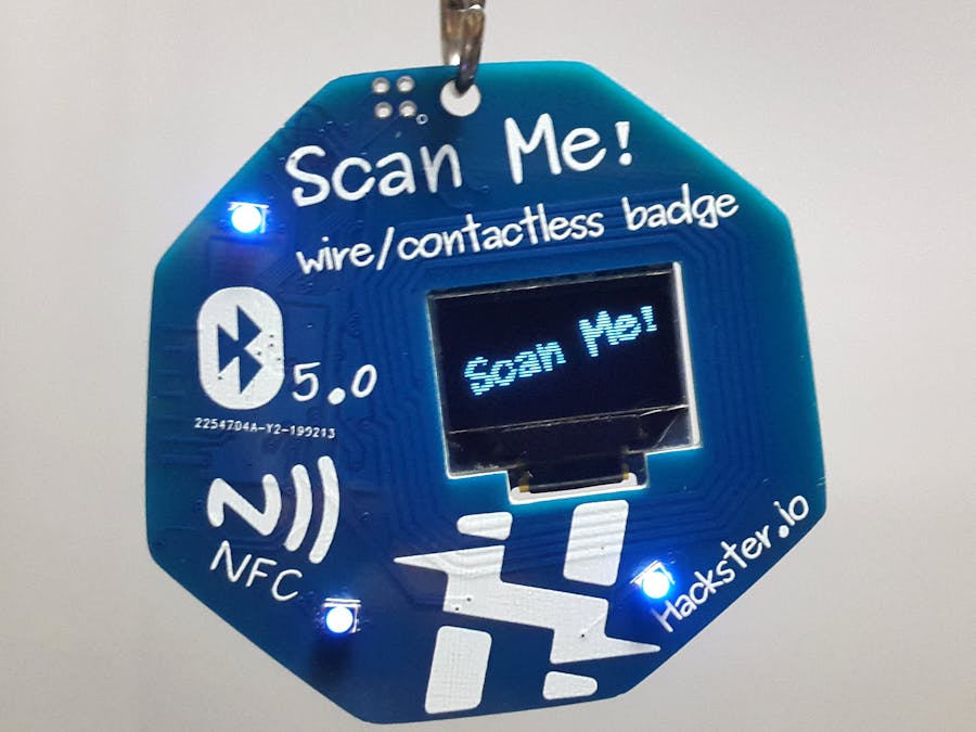
In this project I will present the build of the Scan Me! badge, a low power wire / contactless badge, with Bluetooth Low Energy 5.0 and NFC functionality.
The badge is based on the Nordic nRF52832, a low power RF SoC featuring BLE 5.0 connectivity, NFC tag emulation and a powerful Arm Cortex-M4 processor.
The main features of the badge are:
- BLE connectivity
- NFC tag emulation
- Arm Cortex-M4 @ 64Mhz
- OLED screen
- 3 x RGB LED-s
- 2 x user buttons
- low power usage - 2+ years from a CR2032 battery
- OTA update over BLE
The project also serves educational purposes. Building such a badge, I think it is a great way to learn more about things like BLE, NFC or low power design.
Electrical DesignTo do the electrical and PCB design, I used the KiCad EDA Open Source Electronics Design Automation Suite.
(sorry Eagle team, KiCad is better for hobby and open source projects :D)
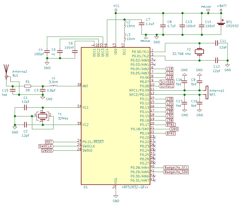
The base schematics is is based on the 53.3 Schematic QFAA QFN48 with DC/DC regulator and NFC setup reference from the Nordic nRF52832's datasheet.
Components:
- Nordic nRF52832 SoC (U1) - the main SoC, the "brain" of the badge
- 32 MHz Crystal Oscillator (Y1) - used to generate the main 64 MHz system clock
- 32.768 kHz Crystal Oscillator (Y2) - used for time keeping (
delay()function, etc.) - DC/DC converter external components - 2 inductors (L2, L3) + a capacitor (C7) - these are needed as, to reduce the power consumption, we will use the built in DC / DC converter (instead of the LDO regulator)
- BLE 2.4Ghz Radio - 2.4 GHz antenna (Antenna2) + a couple of components for impedance matching and calibration (L1, C3, R1, C15)
- NFC Antenna (Antenna1) + capacitors for antenna tuning (C9, C10 C16, C17)
- Power - CR2032 battery, capacitors (C4 C5, C6, C7, C8, C13, C14)
Along the main components, I also added some peripherals:
- 1 x OLED Screen - 4 pin connector (J2): GND, VCC, SCL, SDA - we will use an I2C OLED module like this
- 3 x RGB LED (D1, D2, D3) - 4 pin, common anode configuration
- 2 x Push Button (SW1, SW2) - active low - the pull-ups for the corresponding GPIO pins must be activated
Also added the some connectors:
- #BadgeLife Shitty Add-On Connector (X1) - to be used with Shitty Add-On-s
- Programming Port (J1) - SWD interface for programming the board
The exact components and footprints were select on a "on-the-fly" basis:
- for the 2.4GHz antenna I ended up using a Texas Instruments SWRA117D PCB antenna (I choose this mainly because it's small size and because it is already present in KiCad's built in library)
- the NFC antenna is just a hand drawn PCB traces
- for resistors, capacitor and inductors I just assigned SMD 0805 and looked up the components afterwards
- the RGB LEDs, switches, crystals first I choose from the LCSC catalog, then I assigned the appropriate footprints
- the OLED screen I already had
For the full list of the components, see the BOM file in the attachments.
"Artwork"The first sketches of the badge I made in a notebook. After that, I used Inkscape to do some drawings:
and ended up with this:
To be able to use these drawing in KiCad, I used the svg2mod script from mtl to export SVG file to a KiCad PCB footprint module file (.mod).
To get an usable result, first Objects and Strokes must be converted to Paths. Also, the drawing must be structured with layers associated with KiCad PCB layers: Cu, SilkS, etc. (more on this in the svg2mod's readme).
PCB DesignThe PBC design was done in KiCad Pcbnew:
The first step was to import the Inkscape drawings exported as KiCad module.
After this, I just placed components, starting with the biggest components (battery holder, SoC) and then the smallest ones close to pin they need to connect.
The final layout looks like this:
The NFC Antenna is just "coil" built from a long hand drawn PCB:
2.4 GHz Antenna (BLE) section uses the Texas Instruments SWRA117D PCB antenna. The layout, I think, it can be done better (did not really followed the reference design for the datasheet), but it works (signal strength could be better):
Here are some renders from the KiCad's 3D viewer:
I took into consideration multiple options (OSH Park, JLCPCB, PCBWay) to manufacture the PCB. Finally, I choose JLCPCB because it also offers components (LCSC) and the fast shipping (DHL) at a good price.
It took around 10 days (3 days manufacturing + 7 shipping) to get the PCBs and the components.
I ordered the PCB-s in 2 colors: blue and green. They came out nice, I think:
I also ordered most of the components (all except the OLED Screen and some SMD resistors and capacitors) from LCSC. The total cost for the PCB ($15) and components ($15.84) was $30.84, including DHL shipping.
The soldering of the components it's not super easy, but I think it was doable.
The trick part was to solder the nRF52832 (QFN48 package). I used the technique from this video. It it done with standard solder and a hot air gun. After soldering, I checked the joints with a microscope (just a cheap USB one).
The rest of the part (mainly 0805 SMD) are easily solderable.
The OLED screen is also SMD soldered. First, I removed the pin header from the module. Then, I filled up the holes with solder and using the soldering iron I soldered the module to the pads from the badge.
Here is how the assembled badge looks like:
(a.k.a. the "I have NO idea what I'm doing!" part)
According to the nRF52832's datasheet, the NFC and BLE antennas needs to be tunned.
The NFC antenna needs to be tunned to 13.56 MHz. A couple of capacitors (in my design C9, C10 C16, C17) are used for this purpose.
There two ways to determine the tuning capacitor (Ctune) values:
- measure (or estimate) the antenna inductance and calculate the capacitor values using the formula from the datasheet
- try different capacitor values, use a network analyzer to measure the resonant frequency of the system
As I did not had access to a network analyzer, I tough to measure the inductance of the antenna. After a couple of tries of measuring the inductance with an Arduino based inductance meter (most of the multi-meters can't measure inductance), I gave up this idea. The inductance of the antenna is expected to be pretty small (in the 1-3uH range), which is not trivial to measure.
So, in the ended up using some online tools to estimate the inductance of the PCB antenna, based on a couple of parameters (height, width, turns, track width, spacing). I tried two of too and they gave the following values:
Applying the two values to the datasheet formula gave me that the 133pF (2.0uH) -> 141pF (1.9uH) capacitance range should be used to tune the antenna to 13.56 MHz. A I had 2 pads for the capacitors (per pin), I ended up using 100pF + 33pF caps.
The impedance of the BLE 2.4GHz Antenna should be matched to 50 Ohm. The L1 and C3 from the base design should do this, but I think, I made the mistake to do not follow the PCB layout recommendation from the datasheet:
In the schematics, I also added a capacitor (C15) for fine tuning, but this ended up not populated.
The antenna works, but the signal strength could be better, I think.
It seems that a really Vector Network Analyzer is really needed to do this properly.(The topic sounds interesting, so I may end up getting a one :) )
SoftwareThe board can be programmed in Arduino IDE, after installing some board packages and libraries.
To add support for nRF5x boards we can install in the Boards Manager, the arduino-nRF5 package from sandeepmistry. Then we can use the Generic nRF52 board to program the badge:
The arduino-nRF5 package do not has support for the NFC functionality. Fortunately, the arduino-core-nrf52 package from arduino-org had it, so I ported it to a my fork of the arduino-nRF5. The code is uploaded to bluetiger9/arduino-nRF5, branch NFC. (The changes got a little bit messy :D, so I did no submit a pull request yet)
The NFC library provides methods to:
- set a Text to be published
- set an URL to be published
- set an Android APP to be launched
The BLE functionality is provided by the arduino-BLEPeripheral library, also from sandeepmistry. The library add support for implementing different kind of BLE service / devices. We will mainly use the BLESerial service from the "serial" example.
To explore the power saving features of the nRF52832, I used. Arduino_nRF5x_lowPower library from mristau. The library can be used to:
- switch from the LDO regulator to the DC / DC converter (needs external components) - this reduces the power usage with about 40-50%
- mode Low Power mode and Power Off modes - this reduces the power usage to about a couple of micro-amps - the SoC can be configured to wake on different events: GPIO, NFC field (only GPIO is implemented)
The measured current consumption of the board are as follow:(+theoreticalrun-time froma 200mAhCR2032 battery)
- LDO regulator - 5.35 mA (1.5 days)
- DC / DC converter - 2.82 mA (3 days)
- Power Off mode + wake up on GPIO - 9.7 uA (2+ years)
I also built a simple Demo Application to demonstrate the badge's features. The app has following functionality:
- NFC tag emulation with custom Test, URL
- OLED screen demo
- simple BLE interface to set the Text or URL published by the NFC tag
- after 10 seconds on inactivity, the badge enters power saving mode
I tested the NFC functionality both with an Android Phone (NFC Tools app) and an Arduino RFID reader.
For the BLE functionality I used the nRF UART app from Nordic:
This application can be easily extended with additional functionality.
The source code can be found in the attached repository.
Programming the boardThe nRF52832 SoC can be programmed using the Serial Wire Debug (SWD) protocol. A SWD programmer, like the $3 ST-Link V2 clone from Aliexpress, are needed to do this.
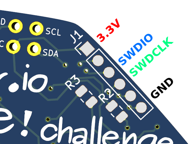
The board has the SWDIO, SWDCLK, SWO, RST, VCC and GND pins of the nRF52832 routed to 6 pads on one the side of the badge:
To program the board we need to connect GND, SWDCLK, SWDIO and VCC to the corresponding pins of the SWD programmer.
There are two ways to do this:
- solder some wires directly on the pads - I did this for the first tests
- hack a programming adapter - I used a spare badge PCB, some spring loaded contact pins, M3 screws and some hot glue:
A further, much better version could be also build from this style of programmer.
OTA UpdateIt would be useful to have the possibility to program the badge wirelessly.
After some research, I found two possible ways to implement the OTA Update:
- using Arduino IDEOTA with IPv6 implemented over BLE
- using the Nordic's Secure DFU bootloader with a new Arduino IDE upload tool
I think, the first variant should be the way to go. It uses the somewhat standard OTA functionality of the Arduino IDE and having IPv6 implemented over BLE could be also useful for other projects too.
Have fun!
Note: I have a couple of unused PCBs for the badge. Drop me a message if you want one.


_4YUDWziWQ8.png?auto=compress%2Cformat&w=48&h=48&fit=fill&bg=ffffff)


_Ujn5WoVOOu.png?auto=compress%2Cformat&w=40&h=40&fit=fillmax&bg=fff&dpr=2)

Comments
Please log in or sign up to comment.