


Hardware components | ||||||
| × | 1 | ||||
Software apps and online services | ||||||
 |
| |||||
The Code Examples demonstrate two special configurations of using the Filter Component available in PSoC Creator. The first Code Example shows how the Filter can be configured for 16 bit signed operations and the second code example shows the operation for full 24 bit filtering.
OverviewPSoC 3 and PSoC 5LP devices have an internal Digital Filter Block (DFB) with which numerous filter designs can be made. PSoC Creator provides a component called Filter with which the filter designs can be accomplished easily.
The Code Examples demonstrate how an analog signal with varying frequencies can be filtered using the Filter component with two different operating modes.
Requirements- Design Tool: PSoC Creator 3.3 SP1 and above
- Programming Language: C (ARM GCC 4.9-2015-q1-update – included with PSoC Creator)
- Associated Devices: All PSoC 3 and PSoC 5LP devices
- Required Hardware: CY8CKIT – 030 PSoC 3 Development Kit, CY8CKIT – 050 PSoC 5LP Development Kit
The project can be tested on the CY8CKIT-050 PSoC 5LP Development Kit. You also need to use a Function generator to feed a sinusoidal signal to the ADC Input and can observe the filtered output on an oscilloscope.
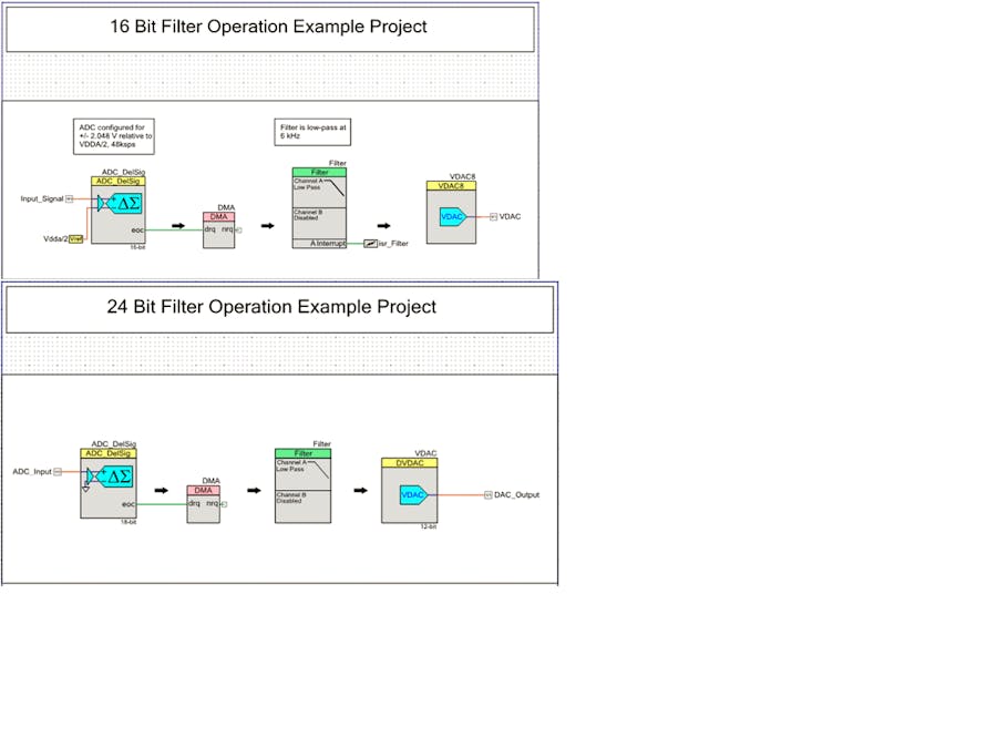
Project 1 – 16 Bit FilterThis project demonstrates digital filtering of 16 bit ADC data using the Digital Filter block in PSoC 5LP. Analog signal is fed to ADC with a resolution of 16 bits. After every end of conversion (eoc) of ADC, DMA transfers the ADC result to the filter’s staging register. Filter is configured as a low pass filter with a cutoff frequency of 6 KHz. An interrupt will be triggered after filtering every input sample. In this interrupt, filtered data is read and is reconstructed to analog domain using VDAC. Since the VADC is 8 bit, only the higher 8 bits of the filtered data is written to VDAC.
Note: PSoC Creator offers Code Example for 8 bit Signed Filter Operation. For 16 bit signed operations, users need to take care of:
Alignment when using DMA:The ADC is MSB aligned to OUTSAMPM, whereas the DFB is aligned to its MSB. i.e., STAGEAH. In this scenario, the DFB will not recognize that a valid data has been placed in its Staging register, since the STAGEAH register is never written. The data align feature allows the received 16-bit data to be internally seen by the DFB in STAGEAH and STAGEAM instead of STAGEAM and STAGEA. Therefore a single DMA transaction from the ADC is sufficient for the DFB to recognize that a valid word has been received.
Similarly, when retrieving the data from the Holding register, the data alignment feature shifts the 16-bit word down to HOLDAM and HOLDA so that a single DMA transaction can move the data to its destination.
Filter CoherencyHere, the coherency of both Staging and Holding Register is set to the middle Byte.
PSoC Creator SchematicHere for demonstration purpose, we are only taking 8 bits from the Filter Holding Register and writing it to the DAC. It is also possible for users to read the full 16 bit output from the Holding Register using Filter Read APIs and store in SRAM arrays if additional processing is required on the filter output.
Build and ProgramBuild the project and program it to the PSoC 5LP Development Kit. Ensure that you set VDDA = VDDD = 5V in the Development Kit (J10 and J11 Jumpers in 5V Position).
Now feed a sinusoidal signal to the Pin P0[0]. Ensure that the sine wave voltage is in the range of 0 – 5 V. The signal should be applied with a Positive Offset as PSoC GPIO Pin cannot accept a voltage which is less than VSSA. Give frequencies in the range of 1 Hz to 10 KHz and observe the DAC Ouptut at Pin P0[7].
As the filter is configured to be a Low Pass Filter with 6 KHz cut-off frequency, you can see the amplitude of signal getting attenuated for input frequencies above 6 KHz.
Note:The projects currently use the PSoC 5LP device. The projects can be easily migrated to PSoC 3 device by just changing the device to PSoC 3 (Right Click Project Name -> Device Selector -> Select Default Device -> PSoC 3). After doing this, the project can be programmed on to the PSoC 3 Development Kit as well.
ResultsInput frequency = 1 KHz
Input frequency = 6 KHz.
Input Frequency = 6.5 KHz
This project demonstrates digital filtering of 24 bit ADC data using the Digital Filter block in PSoC 5LP. Analog signal is fed to ADC with a resolution of 18 bits. After every end of conversion (eoc) of ADC, DMA transfers the ADC result to the filter’s staging register. Filter is configured as a low pass filter with a cutoff frequency of 250 Hz. Filtered data is read and is reconstructed to analog domain using Dithered VDAC. Since dithered VDAC is 12 bit with a maximum value of 0xFF0, only the higher 13 bits of the filtered data is written to VDAC by ignoring the MSB sign bit and saturate the output if the filtered value is more than 0xFF0.
PSoC Creator SchematicNote: Since we are doing 3 byte transfers using DMA, we need to increment the source and destination address as the peripheral is of 16 bit Spoke Width.
Build and ProgramBuild the project and program it to the PSoC 5LP Development Kit. Ensure that you set VDDA = VDDD = 5V in the Development Kit (J10 and J11 Jumpers in 5V Position).
Now feed a sinusoidal signal to the Pin P0[0]. Ensure that the sine wave voltage is in the range of 0 – 5 V. The signal should be applied with a Positive Offset as PSoC GPIO Pin cannot accept a voltage which is less than VSSA. Give frequencies in the range of 1 Hz to 1 KHz and observe the DAC Ouptut at Pin P0[7].
As the filter is configured to be a Low Pass Filter with 250 Hz cut-off frequency, you can see the amplitude of signal getting attenuated for input frequencies above 250 Hz.
ResultsInput frequency = 100 Hz.
Input frequency = 250 Hz
Input Frequency = 280 Hz


Comments
Please log in or sign up to comment.