


FPGA chemistry
Chemical reactions are often modeled as continuous differential equations with reaction rates related to chemical concentrations (law of mass action). As many have pointed out (e.g., Gillespie, Lok, Salwinski and Eisenberg, or Keane, et.al.) reactions actually occur as discrete events involving molecules. The reaction has some probability of occuring, but either occurs, or does not. Thus we replace concentrations with counting individual molecules and differential equations with rolling the dice to see if a reaction occurs. For a bimolecular reaction involving two molecules A and B, with concentrations [A] and [B] and a rate constant K, the probability of the reaction occuring (from mass action) will be K[A][B] . Assuming a time step which is short enough to make the probability of reaction small during the step, the mass action probability is equal to the probability ([A]>randA && [B]>randB && K>randK).
For a bimolecular reaction
involving two molecules A and B, with concentrations [A] and [B] and a rate
constant K, the probability of the reaction occuring (from mass action) will
be K[A][B] . Assuming a time step which is short enough to make
the probability of reaction small during the step, the mass action probability
is equal to the probability ([A]>randA && [B]>randB && K>randK). Where && is
the logical and operation, and randA, randB and randK are
uniform-distribution random numbers (Salwinski and Eisenberg and Keane, et.al.).
We can therefore replace the expensive multiplies with inexpensive logical
operations and random number generation. Random numbers were generated using
a linear
feedback shift register technique. The shift register length was chosen
so that only one xor operation was needed.
The first reaction scheme I implemented is a slightly expanded version of the system presented in Salwinski and Eisenberg. Expansions were the ability of several update events to occur for a given molecular species (as in Keane, et.al.). Examples are below. Each chemical concentration is represented by a 16-bit integer. Each reaction path can increment (+1), decrement (-1), or not change the integer concentration of a chemical at each time step. The restriction of only simple increment/decreement means that reaction probabilities must be adjusted so that the likelyhood of changing the chemical concentration by two or more is negligible. In practice the probability of reaction is set to less than 0.01, so that the probability of two events occuring is less than 0.0001. Salwinski and Eisenberg limited the update so that only one reaction could update any chemical at any time step. I added a queue so that several reactions can update a chemical at each time step. The advantage of my scheme is simpler reaction control, the disadvantage is a longer state machine on each time step. Each time step is seven clock cycles, allowing six inc/dec inputs per chemical per time step.
More generally, what we are doing here is approximating a truncated Poisson distribution of reaction events. We can make a better approximation by allowing concentrations to change by more than +1/-1. Let's say that we make the criterion that our approximation of the Poisson distribution has to cover 99.99% of the full distribution. Or, put differently, the cumulative sum of the discrete distribution has to be 0.9999 up to the point we truncate. I wrote a matlab program to plot the event number at which the cumulative probability reached 0.999 and 0.9999. The figure (left) shows the results. Keeping only one event per reaction time step limits us to a mean rate of 0.01 at 99.99% capture and about 0.03 at 99.9% event capture. For a mean reaction rate up to about 0.085/time step, keeping up to two events per reaction captures 99.99% of the events. Keeping three events allows reaction rates up to about 0.2/time step (at 99.99% capture). So using the 99.99% criterion, keeping two events instead of one event gives us about an 8-fold speed up, while keeping three events only gives us another factor of two above the two-event rate.
So what do we need to do to implement a maximum of two events? If we model the two reactions as separated in space, and therefore independent, we need to compute the probability of two completely independent reactions separately, then decide if 0, 1 or 2 events occured. If either reaction occurs set the inc/dec outputs to +1/-1. If both occur set the inc/dec outputs to +2/-2. If neither occurs, inc/dec are zero. This seems to be a workable system and was implemented below. A manuscript version of this description is here.
HIgh
quality random number s essential for this scheme to work. It is
possible to parallelize the linear feedback shift register to get more
effective
shits per clock cycle. Hoogland, et.al. describe a high quality random
number generator designed for Ising model simulation. Using this 127-bit
shift register with parallel 16-bit output triples the size of the
reaction module. The following figure is taken from the paper and shows
the parallelized feedback paths of the shift register. The inputs to to
each 8-bit subsection are the xor of the two bits noted at the top of
the column. I have not yet carried out statistical tests to see if the
higher quality random numbers matter for the simulation. The 16-bit
output is taken as bits 97 to 112 from fifteen 8-bit (and one 7-bit)
shift registers. The improved Michaelis–Menten top-level module is here.
The 127-bit generator is overkill for a 16-bit random number (but works
well for 32-bit computed in 2 cycles), so I scaled down the generator
to a 63-bit version with feedback from bits 62 and 63 (one's based). The
parallelized bit layout is the same as in the figure to the left, but
truncated at 4 bits per register.The parallelized version has sixteen
4-bit shift registers loaded in parallel. For instance, on the same
clock cycle,bit62 xor bit63 is shifted into shift register 16, bit61 xor bit62 is shifted into shift register 15, bit48 xor bit49 is shifted into shift register 2, and bit47 xor bit48 is shifted into shift register 1.
The Michaelis–Menten top-level module with 63-bit shift register is here. The Oregonator is here. The Oregonator example uses about 9% of the Altera DE2 board FPGA logic element resources.
The design was extended to include serial output of a waveform so
that a better comparision could be made with the Matlab differential
equation versions. The serial module takes a 16 bit number and converts
it to 4-digit hexadecimal terminated with <crlf> characters so that a call to Matlab fscan(s, '%x') can read it, where s is a serial object. The Michaelis–Menten top-level module with 127-bit shift register and serial is here (project archive). The Matlab code to read the hex is here as is the ODE analysis program (and function).
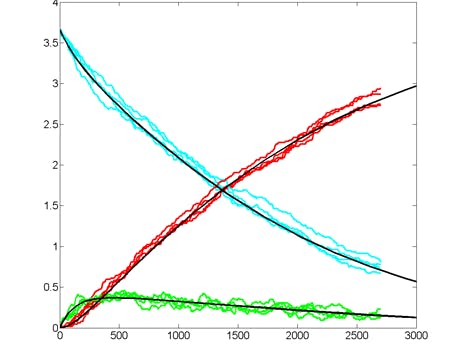
Results for substrate concentrations of 240/2^16 and 4096/2^16 are shown below. Notice the fluctuations are greater for the smaller
number of molecules on the left. The linked Verilog and Matlab programs
are coded for the higher concentration. Black lines are the Matlab
differential equation code, color lines are the FPGA output.
Repeating the stochastic simulations with different random number
seeds yields the following results for the two cases shown above.
The Oregonator with 63-bit random number generator was also modified for serial output (archive). The output was compared to a Matlab simulation of the same stochastic algorithm. The matlab version took 870 seconds
to run on my desk machine (3.2 GHz Core Duo with 8 Gbyte memory) and 8
seconds to run on the FPGA. Note that there are some significant
differences between the two simulation outputs. These diffferences seem
to depend on the random number seed used and so are probably related to
random fluctuations in chemical concentration. Black lines are the
Matlab stochastic code, color lines are the FPGA stochastic output. The
image to the right is the FPGA stochastic simulation compared to an ODE code (and function) in Matlab. In this case the amplitudes seem correct, but the period of the oscillation seems to drift.
References.
John F. Keane, Christopher Bradley, Carl Ebeling, A Compiled Accelerator for Biological Cell Signaling Simulations Cell Systems, International Symposium on Field Programmable Gate Arrays archive Proceedings of the 2004 ACM/SIGDA 12th international symposium on Field programmable gate arrays table of contents Monterey, California, USA SESSION: Pages: 233 - 241, 2004
Salwinski L, Eisenberg D., In silico simulation of biological network dynamics. Nat Biotechnol. 2004 Aug;22(8):1017-9. Epub 2004 Jul 4.
Larry Lok, The need for speed in stochastic simulation , Nature Biotechnology 22, 964 - 965 (2004) doi:10.1038/nbt0804-964
Lok L, Brent R., Automatic generation of cellular reaction networks with Moleculizer 1.0. , Nat Biotechnol. 2005 Jan;23(1):131-6.
D. Gillespie, Exact Stochastic Simulation of Coupled Chemical Reactions, Journal of Physical Chemistry, No. 81, pp. 2340-2361, 1977.
Daniel T. Gillespie, Stochastic Simulation of Chemical Kinetics, Annu. Rev. Phys. Chem. 2007.58:35-55
Hong Li,Yang Cao,Linda R. Petzold, and Daniel T. Gillespie, Algorithms and Software for Stochastic Simulation of Biochemical Reacting Systems, Biotechnol Prog. 2008; 24(1): 56–61. Published online 2007 September 26. doi: 10.1021/bp070255h.
Jürgen Pahle, Biochemical simulations: stochastic, approximate stochastic and hybrid approaches, Brief Bioinform. 2009 January; 10(1): 53–64. Published online 2009 January 16. doi: 10.1093/bib/bbn050.
R. J. Field, R. M. Noyes, Oscillations in Chemical Systems IV. Limit cycle behavior in a model of a real chemical reaction, J. Chem. Phys. 60(1974)1877-84.
A. Hoogland, J. Spaa, B. Selman and A. Compagner, A special-purpose processor for the Monte Carlo simulation of ising spin systems, Journal of Computational Physics, Volume 51, Issue 2, August 1983, Pages 250-260
chem code
// --------------------------------------------------------------------
// --------------------------------------------------------------------
//
//  Major Functions: Oregonator chem simulation
//	With VGA readout -- VGA state is in m4k blocks
//
// 	Chem model from
//		Nature Biotechnol. 2004 Aug;22(8):1017-9. Epub 2004 Jul 4.
//      In silico simulation of biological network dynamics.
//		Salwinski L, Eisenberg D.
//      and
//
// Modify for up to TWO reactions/time step
//
// --------------------------------------------------------------------
//
// Revision History :
// --------------------------------------------------------------------
// Bruce R Land, Cornell University, Jan 2010
// Bruce R Land, Cornell University, Oct 2009
// Improved top module written by Adam Shapiro Oct 2009
// --------------------------------------------------------------------

module DE2_TOP (
    // Clock Input
    input         CLOCK_27,    // 27 MHz
    input         CLOCK_50,    // 50 MHz
    input         EXT_CLOCK,   // External Clock
    // Push Button
    input  [3:0]  KEY,         // Pushbutton[3:0]
    // DPDT Switch
    input  [17:0] SW,          // Toggle Switch[17:0]
    // 7-SEG Display
    output [6:0]  HEX0,        // Seven Segment Digit 0
    output [6:0]  HEX1,        // Seven Segment Digit 1
    output [6:0]  HEX2,        // Seven Segment Digit 2
    output [6:0]  HEX3,        // Seven Segment Digit 3
    output [6:0]  HEX4,        // Seven Segment Digit 4
    output [6:0]  HEX5,        // Seven Segment Digit 5
    output [6:0]  HEX6,        // Seven Segment Digit 6
    output [6:0]  HEX7,        // Seven Segment Digit 7
    // LED
    output [8:0]  LEDG,        // LED Green[8:0]
    output [17:0] LEDR,        // LED Red[17:0]
    // UART
    output        UART_TXD,    // UART Transmitter
    input         UART_RXD,    // UART Receiver
    // IRDA
    output        IRDA_TXD,    // IRDA Transmitter
    input         IRDA_RXD,    // IRDA Receiver
    // SDRAM Interface
    inout  [15:0] DRAM_DQ,     // SDRAM Data bus 16 Bits
    output [11:0] DRAM_ADDR,   // SDRAM Address bus 12 Bits
    output        DRAM_LDQM,   // SDRAM Low-byte Data Mask
    output        DRAM_UDQM,   // SDRAM High-byte Data Mask
    output        DRAM_WE_N,   // SDRAM Write Enable
    output        DRAM_CAS_N,  // SDRAM Column Address Strobe
    output        DRAM_RAS_N,  // SDRAM Row Address Strobe
    output        DRAM_CS_N,   // SDRAM Chip Select
    output        DRAM_BA_0,   // SDRAM Bank Address 0
    output        DRAM_BA_1,   // SDRAM Bank Address 0
    output        DRAM_CLK,    // SDRAM Clock
    output        DRAM_CKE,    // SDRAM Clock Enable
    // Flash Interface
    inout  [7:0]  FL_DQ,       // FLASH Data bus 8 Bits
    output [21:0] FL_ADDR,     // FLASH Address bus 22 Bits
    output        FL_WE_N,     // FLASH Write Enable
    output        FL_RST_N,    // FLASH Reset
    output        FL_OE_N,     // FLASH Output Enable
    output        FL_CE_N,     // FLASH Chip Enable
    // SRAM Interface
    inout  [15:0] SRAM_DQ,     // SRAM Data bus 16 Bits
    output [17:0] SRAM_ADDR,   // SRAM Address bus 18 Bits
    output        SRAM_UB_N,   // SRAM High-byte Data Mask
    output        SRAM_LB_N,   // SRAM Low-byte Data Mask
    output        SRAM_WE_N,   // SRAM Write Enable
    output        SRAM_CE_N,   // SRAM Chip Enable
    output        SRAM_OE_N,   // SRAM Output Enable
    // ISP1362 Interface
    inout  [15:0] OTG_DATA,    // ISP1362 Data bus 16 Bits
    output [1:0]  OTG_ADDR,    // ISP1362 Address 2 Bits
    output        OTG_CS_N,    // ISP1362 Chip Select
    output        OTG_RD_N,    // ISP1362 Write
    output        OTG_WR_N,    // ISP1362 Read
    output        OTG_RST_N,   // ISP1362 Reset
    output        OTG_FSPEED,  // USB Full Speed, 0 = Enable, Z = Disable
    output        OTG_LSPEED,  // USB Low Speed,  0 = Enable, Z = Disable
    input         OTG_INT0,    // ISP1362 Interrupt 0
    input         OTG_INT1,    // ISP1362 Interrupt 1
    input         OTG_DREQ0,   // ISP1362 DMA Request 0
    input         OTG_DREQ1,   // ISP1362 DMA Request 1
    output        OTG_DACK0_N, // ISP1362 DMA Acknowledge 0
    output        OTG_DACK1_N, // ISP1362 DMA Acknowledge 1
    // LCD Module 16X2
    inout  [7:0]  LCD_DATA,    // LCD Data bus 8 bits
    output        LCD_ON,      // LCD Power ON/OFF
    output        LCD_BLON,    // LCD Back Light ON/OFF
    output        LCD_RW,      // LCD Read/Write Select, 0 = Write, 1 = Read
    output        LCD_EN,      // LCD Enable
    output        LCD_RS,      // LCD Command/Data Select, 0 = Command, 1 = Data
    // SD Card Interface
    inout         SD_DAT,      // SD Card Data
    inout         SD_DAT3,     // SD Card Data 3
    inout         SD_CMD,      // SD Card Command Signal
    output        SD_CLK,      // SD Card Clock
    // I2C
    inout         I2C_SDAT,    // I2C Data
    output        I2C_SCLK,    // I2C Clock
    // PS2
    input         PS2_DAT,     // PS2 Data
    input         PS2_CLK,     // PS2 Clock
    // USB JTAG link
    input         TDI,         // CPLD -> FPGA (data in)
    input         TCK,         // CPLD -> FPGA (clk)
    input         TCS,         // CPLD -> FPGA (CS)
    output        TDO,         // FPGA -> CPLD (data out)
    // VGA
    output        VGA_CLK,     // VGA Clock
    output        VGA_HS,      // VGA H_SYNC
    output        VGA_VS,      // VGA V_SYNC
    output        VGA_BLANK,   // VGA BLANK
    output        VGA_SYNC,    // VGA SYNC
    output [9:0]  VGA_R,       // VGA Red[9:0]
    output [9:0]  VGA_G,       // VGA Green[9:0]
    output [9:0]  VGA_B,       // VGA Blue[9:0]
    // Ethernet Interface
    inout  [15:0] ENET_DATA,   // DM9000A DATA bus 16Bits
    output        ENET_CMD,    // DM9000A Command/Data Select, 0 = Command, 1 = Data
    output        ENET_CS_N,   // DM9000A Chip Select
    output        ENET_WR_N,   // DM9000A Write
    output        ENET_RD_N,   // DM9000A Read
    output        ENET_RST_N,  // DM9000A Reset
    input         ENET_INT,    // DM9000A Interrupt
    output        ENET_CLK,    // DM9000A Clock 25 MHz
    // Audio CODEC
    inout         AUD_ADCLRCK, // Audio CODEC ADC LR Clock
    input         AUD_ADCDAT,  // Audio CODEC ADC Data
    inout         AUD_DACLRCK, // Audio CODEC DAC LR Clock
    output        AUD_DACDAT,  // Audio CODEC DAC Data
    inout         AUD_BCLK,    // Audio CODEC Bit-Stream Clock
    output        AUD_XCK,     // Audio CODEC Chip Clock
    // TV Decoder
    input  [7:0]  TD_DATA,     // TV Decoder Data bus 8 bits
    input         TD_HS,       // TV Decoder H_SYNC
    input         TD_VS,       // TV Decoder V_SYNC
    output        TD_RESET,    // TV Decoder Reset
    // GPIO
    inout  [35:0] GPIO_0,      // GPIO Connection 0
    inout  [35:0] GPIO_1       // GPIO Connection 1
);

   //Turn off all displays.
   /*
   assign HEX0 = 7'h7F;
   assign HEX1 = 7'h7F;
   assign HEX2 = 7'h7F;
   assign HEX3 = 7'h7F;
   assign HEX4 = 7'h7F;
   assign HEX5 = 7'h7F;
   assign HEX6 = 7'h7F;
   assign HEX7 = 7'h7F;
   assign LEDR = 18'h0;
  // assign LEDG = 9'h0;
  */

   //Set all GPIO to tri-state.
   assign GPIO_0 = 36'hzzzzzzzzz;
   assign GPIO_1 = 36'hzzzzzzzzz;

   //Disable audio codec.
   //assign AUD_DACDAT = 1'b0;
   //assign AUD_XCK    = 1'b0;

   //Disable DRAM.
   assign DRAM_ADDR  = 12'h0;
   assign DRAM_BA_0  = 1'b0;
   assign DRAM_BA_1  = 1'b0;
   assign DRAM_CAS_N = 1'b1;
   assign DRAM_CKE   = 1'b0;
   assign DRAM_CLK   = 1'b0;
   assign DRAM_CS_N  = 1'b1;
   assign DRAM_DQ    = 16'hzzzz;
   assign DRAM_LDQM  = 1'b0;
   assign DRAM_RAS_N = 1'b1;
   assign DRAM_UDQM  = 1'b0;
   assign DRAM_WE_N  = 1'b1;

   //Disable Ethernet.
   assign ENET_CLK   = 1'b0;
   assign ENET_CS_N  = 1'b1;
   assign ENET_CMD   = 1'b0;
   assign ENET_DATA  = 16'hzzzz;
   assign ENET_RD_N  = 1'b1;
   assign ENET_RST_N = 1'b1;
   assign ENET_WR_N  = 1'b1;

   //Disable flash.
   assign FL_ADDR  = 22'h0;
   assign FL_CE_N  = 1'b1;
   assign FL_DQ    = 8'hzz;
   assign FL_OE_N  = 1'b1;
   assign FL_RST_N = 1'b1;
   assign FL_WE_N  = 1'b1;

   //Disable LCD.
   assign LCD_BLON = 1'b0;
   assign LCD_DATA = 8'hzz;
   assign LCD_EN   = 1'b0;
   assign LCD_ON   = 1'b0;
   assign LCD_RS   = 1'b0;
   assign LCD_RW   = 1'b0;

   //Disable OTG.
   assign OTG_ADDR    = 2'h0;
   assign OTG_CS_N    = 1'b1;
   assign OTG_DACK0_N = 1'b1;
   assign OTG_DACK1_N = 1'b1;
   assign OTG_FSPEED  = 1'b1;
   assign OTG_DATA    = 16'hzzzz;
   assign OTG_LSPEED  = 1'b1;
   assign OTG_RD_N    = 1'b1;
   assign OTG_RST_N   = 1'b1;
   assign OTG_WR_N    = 1'b1;

   //Disable SDRAM.
   assign SD_DAT = 1'bz;
   assign SD_CLK = 1'b0;

   //Disable SRAM.
   assign SRAM_ADDR = 18'h0;
   assign SRAM_CE_N = 1'b1;
   assign SRAM_DQ   = 16'hzzzz;
   assign SRAM_LB_N = 1'b1;
   assign SRAM_OE_N = 1'b1;
   assign SRAM_UB_N = 1'b1;
   assign SRAM_WE_N = 1'b1;

   //Disable VGA.
   /*
   assign VGA_CLK   = 1'b0;
   assign VGA_BLANK = 1'b0;
   assign VGA_SYNC  = 1'b0;
   assign VGA_HS    = 1'b0;
   assign VGA_VS    = 1'b0;
   assign VGA_R     = 10'h0;
   assign VGA_G     = 10'h0;
   assign VGA_B     = 10'h0;
   */

   //Disable all other peripherals.
   //assign I2C_SCLK = 1'b0;
   assign IRDA_TXD = 1'b0;
   //assign TD_RESET = 1'b0;
   assign TDO = 1'b0;
   assign UART_TXD = 1'b0;


wire	VGA_CTRL_CLK;
wire	AUD_CTRL_CLK;
wire	DLY_RST;

assign	TD_RESET	=	1'b1;	//	Allow 27 MHz
assign	AUD_ADCLRCK	=	AUD_DACLRCK;
assign	AUD_XCK		=	AUD_CTRL_CLK;

Reset_Delay			r0	(	.iCLK(CLOCK_50),.oRESET(DLY_RST)	);

wire reaction_clock;
VGA_Audio_PLL 		p1	(	.areset(~DLY_RST),.inclk0(CLOCK_27),
					.c0(VGA_CTRL_CLK),
					.c1(reaction_clock),
					.c2(VGA_CLK)	);


VGA_Controller		u1	(	//	Host Side
							.iCursor_RGB_EN(4'b0111),
							.oAddress(mVGA_ADDR),
							.oCoord_X(Coord_X),
							.oCoord_Y(Coord_Y),
							.iRed(mVGA_R),
							.iGreen(mVGA_G),
							.iBlue(mVGA_B),
							//	VGA Side
							.oVGA_R(VGA_R),
							.oVGA_G(VGA_G),
							.oVGA_B(VGA_B),
							.oVGA_H_SYNC(VGA_HS),
							.oVGA_V_SYNC(VGA_VS),
							.oVGA_SYNC(VGA_SYNC),
							.oVGA_BLANK(VGA_BLANK),
							//	Control Signal
							.iCLK(VGA_CTRL_CLK),
							.iRST_N(DLY_RST)	);

wire [9:0]	mVGA_R;				//memory output to VGA
wire [9:0]	mVGA_G;
wire [9:0]	mVGA_B;
wire [19:0]	mVGA_ADDR;			//video memory address
wire [9:0]  Coord_X, Coord_Y;	//display coods

/////////////////////////////////////////////////
wire reset;
reg [3:0] state;
//wire reaction_clock;
//assign reaction_clock = VGA_CTRL_CLK ;

// reaction state machine reset
assign reset = ~KEY[0];

////////////////////////////////////////////////
/*From megaWizard:
	module vga_buffer (
	address_a, // use a for state machine
	address_b, // use b for VGA refresh
	clock_a,
	clock_b,
	data_a,
	data_b,
	wren_a,
	wren_b,
	q_a,
	q_b);*/
// Show m4k on the VGA
// -- use m4k a for state machine
// -- use m4k b for VGA refresh
wire [3:0] mem_bit ; //current data from m4k to VGA
reg [3:0] disp_bit ; // registered data from m4k to VGA
wire [3:0] state_bit ; // current data from m4k to state machine
reg we ; // write enable for a
reg [17:0] addr_reg ; // for a
reg [3:0] data_reg ; // for a
vga_buffer display(
	.address_a (addr_reg) ,
	.address_b ({Coord_X[9:1],Coord_Y[8:1]}), // vga current address
	.clock_a (VGA_CTRL_CLK),
	.clock_b (VGA_CTRL_CLK),
	.data_a (data_reg),
	.data_b (4'b0000), // never write on port b
	.wren_a (we),
	.wren_b (1'b0), // never write on port b
	.q_a (state_bit),
	.q_b (mem_bit) ); // data used to update VGA

// make the color
assign  mVGA_R = {10{disp_bit[0]}} ;
assign  mVGA_G = {10{disp_bit[1]}} ;
assign  mVGA_B = {10{disp_bit[2]}} ;

always @ (negedge VGA_CTRL_CLK)
begin
	// register the m4k output for better timing on VGA
	// negedge seems to work better than posedge
	disp_bit <= mem_bit;
end

//////////////////////////////////////////////
// state names
// cycling thru the states advances time one step
parameter react_start=4'd0,
		in1=4'd1, in2=4'd2, in3=4'd3, in4=4'd4,
		in0=4'd5, in5=4'd6, in6=4'd7 ;

// cyclic state machine  react -> update concentrations -> react
always @ (posedge reaction_clock) //reaction_clock
begin
	if (reset)		//synch reset assumes KEY0 is held down 1/60 second
	begin
		//clear the screen
		state <= react_start;	//first state in regular state machine
	end

	//begin state machine to run reaction
	else if ( KEY[3])  // KEY3 is pause
	begin
		case(state)
			react_start: state <= in0 ;
			in0: state <= in1 ;
			in1: state <= in2 ;
			in2: state <= in3 ;
			in3: state <= in4 ;
			in4: state <= in5 ;
			in5: state <= in6 ;
			in6:
			begin
				state <= react_start ;
				if (d_state == disp_end)
				begin
					// copy to temp for display
					Y1temp <= A; // copies to ensure sync
					Y2temp <= S;
					Y3temp <= AE;
				end
			end
		endcase //(state)
	end // else if ( KEY[3])
end // always @ (posedge clock)

///////////////////////////////////////////////////
// write the chemical state to the display memory
reg [3:0] d_state;
reg [8:0] x_pos ; // current plotting position
reg last_clk ; // memory for clock synch

// Choose the display chemical scale factor
parameter display_top_bit=7 ; // code will use 8 bits of 16

// clock dependent random number seed
reg [11:0] seed_offset ;

// the display clock
reg [30:0] clock_divider ;
wire display_clock ;
// how many cycles between display points?
parameter disp_slow_down_factor=21; //20

always @ (posedge reaction_clock) //
begin
	clock_divider <= clock_divider + 1;
	seed_offset = seed_offset + 1;
end
assign display_clock = clock_divider[disp_slow_down_factor];

// state names
parameter disp1=1, disp2=2, disp3=3,
		disp4=4, disp5=5, disp6=6,
		disp7=7, disp8=8, disp9=9,
		disp_end=15;

reg [15:0] Y1temp, Y2temp, Y3temp;
always @(posedge VGA_CTRL_CLK) //VGA_CTRL_CLK
begin
	if (reset | ~KEY[1])		//synch reset assumes KEY0 is held down 1/60 second
	begin
		//clear the screen
		addr_reg <= {Coord_X[9:1],Coord_Y[8:1]} ;	// [17:0]
		we <= 1'b1;							//write some memory
		data_reg <= 4'b0;					//write all zeros (black)
		d_state <= disp_end ;	//wait state in display state machine
		x_pos <= 9'd1 ; //x and y are 9 bit
	end

	else //not reset
	begin
		case(d_state)

			disp1:
			begin
				we <= 1'b0 ;
				addr_reg <= {x_pos,
				   8'd239-Y1temp[display_top_bit:display_top_bit-7]} ;	//(x,y)
				//write a red dot
				data_reg <= 4'b0001 ;
				d_state <= disp2 ;
			end

			disp2:
			begin
				we <= 1'b1;
				//write a red dot
				data_reg <= 4'b0001 ;
				d_state <= disp3 ;
			end

			disp3:
			// finish write a single dot
			begin
				we <= 1'b0;
				d_state <= disp4 ;
			end

			disp4:
			begin
				we <= 1'b0 ;
				addr_reg <= {x_pos, 8'd239-Y2temp[display_top_bit:display_top_bit-7]} ;	//(x,y)
				//write a green dot
				data_reg <= 4'b0010 ;
				d_state <= disp5 ;
			end

			disp5:
			begin
				we <= 1'b1;
				//write a green dot
				data_reg <= 4'b0010 ;
				d_state <= disp6 ;
			end

			disp6:
			// finish write a single dot
			begin
				we <= 1'b0;
				d_state <= disp7 ;
			end

			disp7:
			begin
				we <= 1'b0 ;
				addr_reg <= {x_pos, 8'd239-Y3temp[display_top_bit:display_top_bit-7]} ;	//(x,y)
				//write a blue dot
				data_reg <= 4'b0011 ;
				d_state <= disp8 ;
			end

			disp8:
			begin
				we <= 1'b1;
				//write a cyan dot
				data_reg <= 4'b0011 ;
				d_state <= disp9 ;
			end

			disp9:
			// finish write a single dot
			begin
				we <= 1'b0;
				d_state <= disp_end ;
			end

			disp_end:
			begin
				// wait for the disp clock and one-shot it
				if (display_clock && last_clk==1)
				begin
					d_state <= disp1 ;
					if (x_pos < 9'd320)
						x_pos <= x_pos + 1;
					last_clk <= 1'h0 ;
				end
				// reset the one-shot memory
				else if (~display_clock && last_clk==0)
				begin
					last_clk <= 1'h1 ;
					//Y1temp <= Y1; // copies to ensure sync
					//Y2temp <= Y2;
					//Y3temp <= Y3;
				end
			end
		endcase //(d_state)
	end

end // display

// Michaelis and Menten ////////////////////////////////
////////////////////////////////////////////////////////
// define A + E <-> AE -> S + E  (enzyme reaction)
// such that 2A can convert to S and S can convert to 2A.

wire [15:0] A, S, AE, E ; // concentrations
// concentration inc/dec from reactions
wire [2:0] AtoAE_inc, AtoAE_dec,
			AEtoA_inc, AEtoA_dec,
			AEtoS_inc, AEtoS_dec;

// define the chemicals.
parameter no_chem = 16'hffff, no_inc = 3'b000 ;

chemical chem_A( A, 16'd240,
			AtoAE_dec, AEtoA_inc,
			no_inc, no_inc,
			no_inc, no_inc,
			state, reaction_clock, reset);

chemical chem_S( S, 16'h0000,
			AEtoS_inc, no_inc,
			no_inc, no_inc,
			no_inc, no_inc,
			state, reaction_clock, reset);

chemical chem_E( E, 16'd60,
			AtoAE_dec, AEtoA_inc, AEtoS_inc, no_inc,
			no_inc, no_inc,
			state, reaction_clock, reset);

chemical chem_AE( AE, 16'h0000,
			AtoAE_inc, AEtoA_dec, AEtoS_dec, no_inc,
			no_inc, no_inc,
			state, reaction_clock, reset);

// define the forward and backward reactions
// inc/dec output signals are nonzero
// if the reaction occurs
// unused concentration inputs should be set to 16'hffff
reaction AtoAE(AtoAE_inc, AtoAE_dec, A, E, 16'hffff,
			state, reaction_clock, reset, 128'h54555555+seed_offset);

reaction AEtoA(AEtoA_inc, AEtoA_dec, AE, no_chem, 16'h0010,
			state, reaction_clock, reset, 128'h55555555+seed_offset);

reaction AEtoS(AEtoS_inc, AEtoS_dec, AE, no_chem, 16'd256,
			state, reaction_clock, reset, 128'h53555555+seed_offset);

//////////////////////////////////////////////////////////
// read out the concentrations
/*
wire [15:0] readout ;
assign readout = (SW[0])? Y3 : Y1 ;
HexDigit Digit0(HEX0, readout[3:0]);
HexDigit Digit1(HEX1, readout[7:4]);
HexDigit Digit2(HEX2, readout[11:8]);
HexDigit Digit3(HEX3, readout[15:12]);

// read out the concentrations
HexDigit Digit4(HEX4, Y2[3:0]);
HexDigit Digit5(HEX5, Y2[7:4]);
HexDigit Digit6(HEX6, Y2[11:8]);
HexDigit Digit7(HEX7, Y2[15:12]);
*/
// visual indication of reactions occuring
//wire LED1_state, LED2_state ;
//assign LED1_state = (X1_Y2_to_Y1_inc == 3'b001)? ~LED1_state:LED1_state ;
//assign LED2_state = (X1_Y2_to_Y1_inc == 3'b011)? ~LED2_state:LED2_state ;
//assign LEDG[1] = LED1_state ;
//assign LEDG[2] = LED2_state ;
endmodule //top module

/////////////////////////////////////////////////////////
// chemical definition module
/////////////////////////////////////////////////////////
// Define chemical:
// Specify the initial concentration
// Produces the current concentration
// Takes up to 6 inc-dec commands to change current concentration
//
module chemical(
		concentration_out,
		init_concentration_in,
		// inc/dec inputs from reaction module
		react_in1, react_in2, react_in3, react_in4, react_in5, react_in6,
		state_in, clock_in, reset_in);

output reg [15:0] concentration_out ;
input wire [15:0] init_concentration_in ; //initial value
input wire [3:0] state_in ;
input wire clock_in, reset_in ;
// react inputs have value 001=+1, 010=+2, 101=-1, 110=-2,
// all others ==no change
parameter plus1=3'b001, plus2=3'b011, minus1=3'b101, minus2=3'b111;
// unused inputs should be set to 3'b000
input wire [2:0] react_in1, react_in2, react_in3, react_in4, react_in5, react_in6;

//state names
parameter react_start=4'd0,
		in1=4'd1, in2=4'd2, in3=4'd3, in4=4'd4,
		in5=4'd6, in6=4'd7, in0=4'd5 ;

// concentration update logic
// choose which of 4 inputs to use
reg [2:0] react_op ; //current reaction operation (+1,+2,-1,-2,none)
reg [15:0] new_concentration;
always @ (*)
begin
	case(state_in)
			//react_start: react_op = react_in1 ;
			in1: react_op = react_in1 ;
			in2: react_op = react_in2 ;
			in3: react_op = react_in3 ;
			in4: react_op = react_in4 ;
			in5: react_op = react_in5 ;
			in6: react_op = react_in6 ;
			default: react_op = 3'b000  ;
	endcase
end
// chemical count update, once for each reaction input
always @(*)
begin
	case(react_op)
		plus1: new_concentration = concentration_out + 16'd1;
		plus2: new_concentration = concentration_out + 16'd2;
		minus1:
		begin
			if (concentration_out > 0)
			    new_concentration = concentration_out - 16'd1;
			else
				new_concentration = concentration_out;
		end
		minus2:
		begin
			if (concentration_out > 1)
			    new_concentration = concentration_out - 16'd2;
			else
				new_concentration = concentration_out;
		end
		default: new_concentration = concentration_out; //no change
	endcase
end
// compute the new reaction output by comparing
// the concentration and a random number
// to allow reaction to occur
//assign react_out = (concentration_out > x_rand[29:14]) ;

always @ (posedge clock_in)
begin

	if (reset_in)
	begin
		concentration_out <= init_concentration_in ;
	end

	// state machine to run reactions
	else
	begin
		// update the chem comparison rand #
		case(state_in)
			in1: concentration_out <= new_concentration ;
			in2: concentration_out <= new_concentration ;
			in3: concentration_out <= new_concentration ;
			in4: concentration_out <= new_concentration ;
			in5: concentration_out <= new_concentration ;
			in6: concentration_out <= new_concentration ;
			default: concentration_out <= concentration_out ;
		endcase
	end // else not reset condition
end // always @ (posedge clock_in)
endmodule

///////////////////////////////////////////////////////////
// reaction definition module
///////////////////////////////////////////////////////////
// Define reaction:
// Specify the reaction rate constnat
// Produces a reaction-occurred inc/dec commands
// Takes up to 2 reaction-allowed commands from chemicals
// The probability of reaction
// (product of (concentrations) x (reaction rate constant))
// MUST be less than 0.01 per time step
//
module reaction(
		inc_out, dec_out,
		chemical_conc_in1,
		chemical_conc_in2,
		reaction_constant_in,
		state_in, clock_in, reset_in, seed_in) ;
// command to chemical to increase/decrease concentration
output wire [2:0] inc_out, dec_out ;
// command from chemical to cause reaction
// unused inputs should be set to 1'b1
input wire [15:0] chemical_conc_in1, chemical_conc_in2;
// rate constant
input wire [15:0] reaction_constant_in ;
// the clocks and stuff
input wire [3:0] state_in ;
input wire clock_in, reset_in ;
input wire [126:0] seed_in;

//state names
parameter react_start=4'd0, in1=4'd1, in2=4'd2, in3=4'd3,
		in4=4'd4, in0=4'd5, in5=4'd6, in6=4'd7 ;

// react inputs have value 001=+1, 010=+2, 101=-1, 110=-2,
// all others ==no change
//parameter plus1=001, plus2=010, minus1=101, minus2=110;

//output from random number gen
wire [15:0] c1_rand1, c2_rand1, k_rand1 ;
wire [15:0] c1_rand2, c2_rand2, k_rand2 ;

//seed to random number gen
reg [126:0] c1_rand1_seed, c2_rand1_seed, k_rand1_seed ;
reg [126:0] c1_rand2_seed, c2_rand2_seed, k_rand2_seed ;

// define rand num gen
// rand127(rand_out, seed_in, state_in, clock_in, reset_in)
rand127 p1(c1_rand1, c1_rand1_seed, state_in, clock_in, reset_in);
rand127 p2(c2_rand1, c2_rand1_seed, state_in, clock_in, reset_in);
rand127 p3(k_rand1, k_rand1_seed, state_in, clock_in, reset_in);
rand127 p4(c1_rand2, c1_rand2_seed, state_in, clock_in, reset_in);
rand127 p5(c2_rand2, c2_rand2_seed, state_in, clock_in, reset_in);
rand127 p6(k_rand2, k_rand2_seed, state_in, clock_in, reset_in);

// logic for determining the result of a reaction
// if (reaction input 1) and (reaction input 2) and
// (reaction constant>rand) then reaction proceeds
// Two events happen if: (rnd<A) & (rnd<(A-1)) & (rnd<B) & (rnd<(B-1)) & (rnd<K) & (rnd<K)
// One event happens if: ((rnd<A) | (rnd<(A))) & ((rnd<B) | (rnd<(B))) & ((rnd<K) | (rnd<K)) & ~(two-events)

wire reaction1_goes, reaction2_goes;

// independent version
assign reaction1_goes =
((chemical_conc_in1 > c1_rand1) &&
(chemical_conc_in2 > c2_rand1) &&
(reaction_constant_in > k_rand1 ))
||
((chemical_conc_in1 > c1_rand2 ) &&
(chemical_conc_in2 > c2_rand2 ) &&
(reaction_constant_in > k_rand2)) ;

// both reactions go
assign reaction2_goes =
(chemical_conc_in1 > c1_rand1 )&&
(chemical_conc_in1 > c1_rand2)&&
(chemical_conc_in2 > c2_rand1)&&
(chemical_conc_in2 > c2_rand2)&&
(reaction_constant_in > k_rand1)&&
(reaction_constant_in > k_rand2) ;

// construct the inc/dec codes
assign inc_out = {1'b0, reaction2_goes, reaction1_goes} ; //reaction2_goes
assign dec_out = {1'b1, reaction2_goes, reaction1_goes} ;

// generate random numbers
always @ (posedge clock_in) //
begin

	if (reset_in)
	begin
		//init random number generators
		c1_rand1_seed <= seed_in ;
		c2_rand1_seed <= seed_in+1000 ;
		k_rand1_seed <= seed_in+2000 ;
		c1_rand2_seed <= seed_in+3000 ;
		c2_rand2_seed <= seed_in+4000 ;
		k_rand2_seed <= seed_in+5000 ;
	end

	// state machine to update rnadom number
	// to compare to reaction constant
	/*
	else
	begin
		//if(state_in == react_start)
		//begin
			//react_out <= (concentration_out > x_rand[29:14]) ;
			c1_rand1 <= {c1_rand1[29:0], c1_low_bit1} ;
			c2_rand1 <= {c2_rand1[29:0], c2_low_bit1} ;
			k_rand1 <= {k_rand1[29:0], k_low_bit1} ;
			c1_rand2 <= {c1_rand2[29:0], c1_low_bit2} ;
			c2_rand2 <= {c2_rand2[29:0], c2_low_bit2} ;
			k_rand2 <= {k_rand2[29:0], k_low_bit2} ;
		//end
	end
	*/
end
endmodule

//////////////////////////////////////////////////////////
// Decode one hex digit for LED 7-seg display
//////////////////////////////////////////////////////////

module HexDigit(segs, num);
	input [3:0] num	;		//the hex digit to be displayed
	output [6:0] segs ;		//actual LED segments
	reg [6:0] segs ;
	always @ (num)
	begin
		case (num)
				4'h0: segs = 7'b1000000;
				4'h1: segs = 7'b1111001;
				4'h2: segs = 7'b0100100;
				4'h3: segs = 7'b0110000;
				4'h4: segs = 7'b0011001;
				4'h5: segs = 7'b0010010;
				4'h6: segs = 7'b0000010;
				4'h7: segs = 7'b1111000;
				4'h8: segs = 7'b0000000;
				4'h9: segs = 7'b0010000;
				4'ha: segs = 7'b0001000;
				4'hb: segs = 7'b0000011;
				4'hc: segs = 7'b1000110;
				4'hd: segs = 7'b0100001;
				4'he: segs = 7'b0000110;
				4'hf: segs = 7'b0001110;
				default segs = 7'b1111111;
		endcase
	end
endmodule


//////////////////////////////////////////////////////////
// 16-bit parallel random number generator ///////////////
//////////////////////////////////////////////////////////
// Algorithm is based on:
// A special-purpose processor for the Monte Carlo simulation of ising spin systems
// A. Hoogland, J. Spaa, B. Selman and A. Compagner
// Journal of Computational Physics
// Volume 51, Issue 2, August 1983, Pages 250-260
//////////////////////////////////////////////////////////
module rand127(rand_out, seed_in, state_in, clock_in, reset_in);
	// 16-bit random number on every cycle
	output wire [15:0] rand_out ;
	// the clocks and stuff
	input wire [3:0] state_in ;
	input wire clock_in, reset_in ;
	input wire [127:1] seed_in; // 128 bits is 32 hex digits 0xffff_ffff_ffff_ffff_ffff_ffff_ffff_ffff

	reg [8:1] sr1, sr2, sr3, sr4, sr5, sr6, sr7, sr8,
				sr9, sr10, sr11, sr12, sr13, sr14, sr15, sr16;

	// state names
	parameter react_start=4'd0 ;

	// generate random numbers
	assign rand_out = {sr1[7], sr2[7], sr3[7], sr4[7],
							sr5[7], sr6[7], sr7[7], sr8[7],
							sr9[7], sr10[7], sr11[7], sr12[7],
							sr13[7], sr14[7], sr15[7], sr16[7]} ;

	always @ (posedge clock_in) //
	begin

		if (reset_in)
		begin
			//init random number generator
			sr1 <= seed_in[8:1] ;
			sr2 <= seed_in[16:9] ;
			sr3 <= seed_in[24:17] ;
			sr4 <= seed_in[32:25] ;
			sr5 <= seed_in[40:33] ;
			sr6 <= seed_in[48:41] ;
			sr7 <= seed_in[56:49] ;
			sr8 <= seed_in[64:57] ;
			sr9 <= seed_in[72:65] ;
			sr10 <= seed_in[80:73] ;
			sr11 <= seed_in[88:81] ;
			sr12 <= seed_in[96:89] ;
			sr13 <= seed_in[104:97] ;
			sr14 <= seed_in[112:105] ;
			sr15 <= seed_in[120:113] ;
			sr16 <= {1'b0,seed_in[127:121]} ;
		end

		// update 127-bit shift register
		// 16 times in parallel
		else
		begin
			if(state_in == react_start)
			begin
				sr1 <= {sr1[7:1], sr1[7]^sr16[7]} ;
				sr2 <= {sr2[7:1], sr2[7]^sr1[8]}  ;
				sr3 <= {sr3[7:1], sr3[7]^sr2[8]}  ;
				sr4 <= {sr4[7:1], sr4[7]^sr3[8]}  ;
				sr5 <= {sr5[7:1], sr5[7]^sr4[8]}  ;
				sr6 <= {sr6[7:1], sr6[7]^sr5[8]}  ;
				sr7 <= {sr7[7:1], sr7[7]^sr6[8]}  ;
				sr8 <= {sr8[7:1], sr8[7]^sr7[8]}  ;
				sr9 <= {sr9[7:1], sr9[7]^sr8[8]}  ;
				sr10 <= {sr10[7:1], sr10[7]^sr9[8]}  ;
				sr11 <= {sr11[7:1], sr11[7]^sr10[8]}  ;
				sr12 <= {sr12[7:1], sr12[7]^sr11[8]}  ;
				sr13 <= {sr13[7:1], sr13[7]^sr12[8]}  ;
				sr14 <= {sr14[7:1], sr14[7]^sr13[8]}  ;
				sr15 <= {sr15[7:1], sr15[7]^sr14[8]}  ;
				sr16 <= {sr16[6:1], sr16[7]^sr15[8]}  ;
			end
		end
	end
endmodule


////////// end of file ////////////////////////// 
Comments
Please log in or sign up to comment.