The idea behind this project concerns the use of CMOS sensors in industrial optical inspection, as an inexpensive alternative to CCD sensors. For instance, some common task that an industrial optical inspection system has to perform are dimensional measurements of various objects on a conveyor belt or error detection (e.g. scratches).
For this project, we aim to create a case study to perform various dimensional measurements, using an inexpensive CMOS sensor, the OV7670 camera module and the Digilent Nexys Video FPGA.
About OV7670The OV7670 camera module is a low voltage CMOS image sensor that provides images in YUV, RGB, GRB formats. For this project we chose to use RGB565 pixel format.
The camera is controlled through the standard Serial Camera Control Bus Interface (SCCB) and operates at up to 30 fps, with a 640 x 480 VGA image array, where pixels are sent as 2 bytes packets.
SCCB interface is compatible with I2C interface, thus allowing manipulation over the camera internal registers from another host. The camera supplies the pixel clock signal (PCLK) and sends data back to the host with synchronize signals such as HREF, VSYNC, HSYNC.
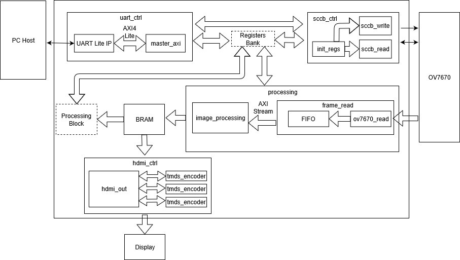
Overall ArchitectureThe overall architecture works as follows:
- As discussed earlier, the OV7670 camera module outputs pixels in the RGB565 format using 2 bytes packets.
- The module frame_read acquires the video data from OV7670 and outputs them as an AXI stream, thus enabling the data to be sent to any image processing module that receives as input the axi stream image. Data is aquired through the ov7670_read module, that is activated after the camera registers are initialized in sccb_ctrl.
- After this, the frame is stored in a FIFO that has a native interface and is generated with FIFO Generator.
- The data stored in FIFO is then converted in an AXI Stream and is ready to be used as input in any module that processes images sent through AXI Stream.
- So far, a module that performs edge detection is available. This module was written using Vivado HLS and unpacks the received data, filters it and than packs it back to an AXI Stream.
- The filtered data is then stored into a block ram with native interface using a intermediate module (axi2bram) that unpacks the AXI Stream image. The BRAM is created using Vivado Block Memory Generator from the IP Catalog.
- HDMI_CTRL reads the data stored in BRAM and sends them to a display through the HDMI port. Data conversions are performed from RGB565 to RGB888, using the 8b/10b TMDS (Transition-minimized differential signaling) encoder.
- The data flow between nexys video and 0V7670 is ensured by the SCCB_CTRL module, which enables for the camera registers to be read/ written and also has initialization values for these registers.
- The SCCB_CTRL module is comprised of three 3 modules: sccb_write and sccb_read that perform read/write operatios on camera registers and init_regs module, that stores initialization values for the registers.
- The UART_CTRL module enables the communication between the Nexys Video board and a PC Host by reading and writing in/from the internal FPGA registers or the camera registers.
- UART_CTRL uses UART Lite from the IP Catalog, controlled by an AXI4 Lite interface
- Using a GUI created with Microsoft Visual Studio, we can control the internal registers of the FPGA or the camera. For the moment, the application can send reading/writing requests through the serial port, using 2 bytes packets and only the OV7670 camera registers can be accessed, as the registers bank is not yet implemented.
Over the next few weeks, the Registers Bank and a second Processing Block ar to be implemented. While the first block serves mainly for filtering the input image, the second one will provide features' extraction.
Finally, this will allow us to perform our test case, in which various dimensional measurements for a simulated set of objects are to be made.


_b3T40wUW0R.png?auto=compress%2Cformat&w=900&h=675&fit=min)


Comments