Stereopsis is the inference of depth by comparing two images from slightly different perspectives. There are a number of local and global algorithms used to obtain a real time stereo depth map.
The computational requirements for stereo however are grow exponentially depending on resolution. Before one delves into the implementation of stereo vision what is needed is a stereo camera setup!
This series will document how to build a stereo camera setup from scratch. The next step will then be to experiment with stereo algorithms
This project will outline the design of a stereo camera platform for a ZYNQ FPGA SOC. The ZC702 development board will be used as the main SOC however the design can be easily ported to any board with an FMC connector that uses the proper voltage CMOS levels for the camera. The first part of the project detail the hardware design setup and Vivado FPGA design for a stereo platform setup
In this case the design will be considerably simplified by keeping both images sources at the same baseline.
Each corresponding feature from the two cameras should be at the same level. This is called rectification. To simplify the rectification process the two cameras will be placed side by side.
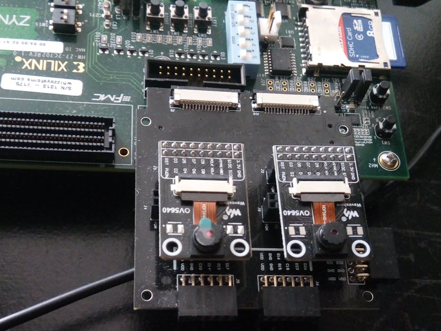
HardwareThe hardware side of this project consists of a ZC702 development board, two OV5640 cameras and one Stereo FMC board.
ZC702
This development board contains a ZYNQ7000 XC7020. It's the same chipset used on PYNQ and Zedboard so the design can be ported quite easily to those development boards.
The ZC702 development board contains XC7020 FPGA SOC. This development board has two LPC (Low Pin count ) FMC (FPGA Mezzanine Card) connectors which bring out a number of pins to the external world.
By default the pins are setups to operate at 2.8V logic level.
DVP OV5640 cameras
For this project I selected DVP cameras since they are easily obtainable. Another advantage is that one can find almost working configuration codes. On the other side thee parallel interface requires 14 pins (16 if including the power pins) so that amounts to 28 pins for a dual camera setup. This is where the FMC comes to play since it bring out a number of pins as differential pair. Looking around for a FMC adapter card shows that there are very few that support a stereo setup.
The Stereo FMC (schematics below) is a mezannine card that allows one to use either DVP or MIPI-CSI cameras with any development board that is equipped with an FMC connector.
Stereo FMC
In this project a stereo FMC card and two cameras were used to build a stereo camera video mixer jig. This setup allows testing stereo algorithms.
The schematics of the stereo FMC card are shown below.
The stereo FMC plugs into one of the two LPC FMC female sockets of the ZC702 board. It is compatible with both 20 pin and 22 pin DVP camera modules such as OV5640, OV7670, OV2640 and so on. Raspberry PI, camera V1, contains an OV5640 sensor configured with a MIPI-CSI interface.
The Stereo card contains 1 dual PMOD connector which was used to connect a VGA PMOD, one single PMOD, two 18 pin DVP camera connectors, two 20 pin DVP camera connectors used for cameras like OV2640 and finally two MIPI-CSI RX camera connectors used for cameras like Raspberry Pi V1 which come with a 15 pin FPC connector.
There are a number of camera interfaces however DVP (Digital Video Port) and MIPI-CSI are two of the main ones.
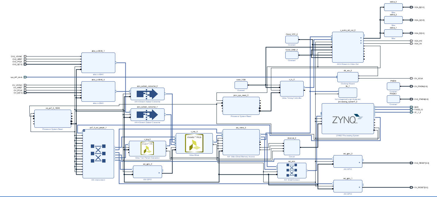
Vivado DesignThe Vivado IP intergrator will be used to build a top level schematic with a video mixer. The output of the video mixer will be sent to the HDMI display.
A number of video blocks from the Vivado library are used as shown below.
VDMA
The VDMA is configured in triple buffer mode. This helps prevent tearing artifacts unlike the case where a single buffer is used. Since the output of the mixer AXI4-Stream data bus has a length of 24bit (8 bits per color), so the stream data width is configured to be 24bits. The line buffer width should be at least the size of the scan-line width. In this case for a 1280x720p resolution a buffer depth of 2048 was used.
Video Mixer.
The video mixer IP is an HDL derived IP block which can take up to 16 video streams. It's interesting to note that IP uses version 4 but the SDK driver is on version 5. There are a couple of important notes with respect to this IP. It needs an external reset which is not clearly mentioned on the user guide.
The SDK driver is also a bit buggy, so one has to modify the underlying BSP driver to get a working setup.
The VTC was configured in generation mode for a resolution of 1280x720p.
VGA output
Finally the AXIS4 to Video in is configured in RGB mode and the parallel vectored video data is wired to a VGA monitor through the FMC card dual PMOD by using a VGA PMOD.
HDMI pipeline
A second version implemented the pipeline to use the on-board HDMI decoder. In that case a color space conversion has to be implemented through the use of the RGB to YCbCr chroma IP (RGB -> YUV444) and then by re-sampling the chroma components from YUV444 to YUV422.
Camera configuration
The main advantages of this FMC are the fact that you can use different DVP cameras (OV7670, OV2640, OV5640) or even two Raspberry Pi V1 cameras with a MIPI-CSI interface.
As image sensors, the OV5640 DVP camera sensor were used. The main reason being the almost open source configuration codes found on the usual websites.
Since the cameras use the SCCB (a clone of I2C) for configuration. to configure both cameras, normally one would use a multiplexer. This FMC card however uses separate pins allocated for each camera.
Clock Synchronization
In a stereo setup, synchronization is another issue that shows up when dealing with the DVP image sensors. Each sensor is fed with a master clock (XCLK). This clock decides the pixel output clock but normally for VGA resolution with these cameras it's around 24Mhz.
To avoid additional synchronization issues on the FPGA the FMC is configured to supply the same XCLK to both cameras. If this was not the case one would have to use FIFOs and manually time the delay from one camera to the next.
The design consists of the Vivado block diagram and the SDK (Vitis) baremetal firmware.
The design including the video mixer utilizes around 1/4 of the FPGA resources.
Vitis SDK design
The design was tested using the bare-metal SDK, implemented in Xilinx SDK or Vitis.
The main steps of the firmware are as follows:
1. First the GPIO peripherals are initialized. The cameras and mixer need an external reset.
2. Second, the I2C peripheral for each camera is initialized. In this design both PS I2C busses are used.
3. The externa I2C switch is then selected from IIC PS1.
4. There are 3 video sources in this setup. The TPG which is used as a canvas for the master layer and the two camera sources.
The TPG is configured first with a 1280p resolution. Next the two cameras are initialized and configured for RGB565 pixel format.
5. The VDMA is configured next. Since the pixels are resized to match with the AXIS stream format of the Video mixer, the VDMA must be configured to use 3 pixels per byte.
6. Since the color space of the mixer is in RGB format and the color space of the HDMI video mixer is in YUV422 format, a color space conversion followed by a chroma re sampling needs to be implemented.
The chroma-resampler IP requires a license however.
Some issues that were encountered due to SDK bugs with the mixer core. Specifically in streaming mode one has to edit the BSP library so that the full window resolution of each layer can be used.
The next step would be to add stereo block matching IP so that a disparity map can be built and add AI tracking capabilities.
ConclusionThis project showed how to build a FPGA stereo camera platform using a ZC702 development board together with the Xilinx Video Mixer IP. The design serves as a testbench for implementing stereo algorithms on the FPGA.


Comments
Please log in or sign up to comment.