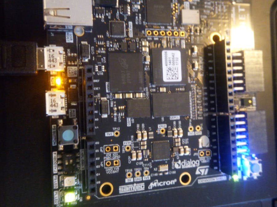
Hey folks! This tutorial will introduce you to the MiniZed Xilinx Zynq development board. We will initially get our feet wet by implementing a simple example that modulates an LED with a PWM circuit.
First let's cover some terminology. Xilinx Zynq is what's called a System on Chip (SoC). The MiniZed ZYNQ 7007 couples a single core ARM processor with an FPGA fabric. The ARM side is called PS (Processing System) while the FPGA is called the PL side (Programmable Logic).
In this tutorial we are going to program the FPGA (PL) to smoothly change the intensity of an LED by using a PWM circuit.
Unlike other SoC's, Zynq devices are tightly integrated so one needs to implement both the PS and PL sides at the same time during the workflow.
1. Installing Vivado and Xilinx SDKStep 1 is to setup the programming environment. To do so one has to download the Vivado SDK 2017.4. Once this is installed launch Vivado.
Vivado is used to implement the hardware system while the Xilinx SDK is used to program the MPU in C/C++.
2. Setting Up the MicroZed Package DefinitionsNow we have to let Vivado know how to recognize the MiniZed board. Out of the box Vivado does not know about this development board so one has to download the MiniZed board definitions file and export those under the boards directory located under the C:\Xilinx folder. After copying the files one has to re-open Vivado. Now when it comes to selecting the parts click the boards button. You'll find that the MiniZed appears automatically. This makes things match easier when setting up a project.
When creating a new project, instead of filtering by parts one just needs to click on boards and select MiniZED.
3. Creating a PWM LED DesignNext step we will create a block diagram with a Zynq system in it.
Once the project is done we'll have to create a schematic with the Zynq SoC in it.
Under IP integrator click on create block design and then click the plus sign.
Search for ZYNQ processing system and then add it to the canvas.
Once you drop a ZYNQ system, click on "Run Block Automation." Then ensure the settings are as below. This will instantiate the ZYNQ core. By default it has two clock outputs and UART/SPI/I2C outputs which we are not using at the moment.
The active low reset and the CLOCK_1 output will be used to drive the PWM module.
4. PWM Controlled LEDIn this section we are going to quickly go over the code. The RTL (Register Transfer Level) code implements a counter. This counter takes a very high frequency clock (50MHz) and outputs a square waveform with a variable duty cycle. This duty cycle is proportional to the intensity of the LED brightness.
module pwmLED(
		input clk,
		input reset_n,
		output PL_LED_G
		);
reg [25:0] count;
reg [7:0] pwm;
always @(posedge clk or negedge reset_n)
	begin
	if(!reset_n) begin
			 count<=0;
			end else begin
   		  count<=count+1;
   		end
	end
wire [6:0] pwm_input = count[25] ? count[24:18] : ~count[24:18];
always @(posedge clk)
begin
   pwm <= pwm[6:0]+pwm_input;
end
assign PL_LED_G = pwm[7];
endmodule
Once we have simulated the Verilog code, we create a new source by naming it pwmLED.v
Vivado allows you to specify the interface I/O graphically.
In this case, however, we can easily do that manually.
5. Setting Up the DesignThe next step is to drag and drop the RTL level file to the schematic. This will create a block diagram with the module interface. Connect the clock output from the Zynq and the active low reset to the PWM module interface. Then right click on the RTL module and export the output pin.
Next step is to click on the design sources and export the top-level wrapper file. Select the bottom option so that Vivado can update the wrapper file if there is any future change.
One can also update the pin name by right clicking on the pin and selecting:
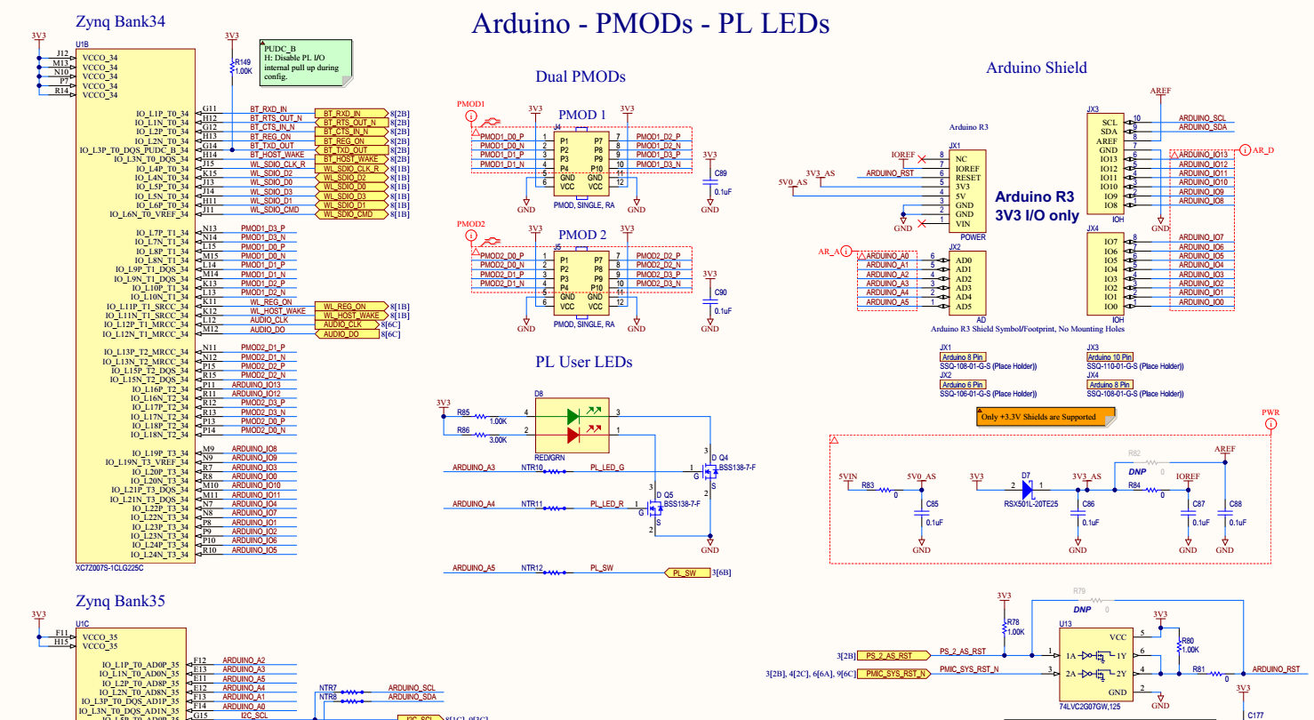
When looking at the board block diagram one can see that the Green LED in the corner is connected directly to the FPGA fabric pins. We are going to use this pin as an output pin in order to connect the FPGA.
To assign pin one uses what's called a constraint file for setting up the voltage levels and instructing the FPGA where to connect the pins of the output model that we are going to code later.
In this step we are going to assign which pin is going to be used from the FPGA side. Create a new constraint file and name it MicroZED_ledPWM.
Now we are going to synthesize the design to a netlist and then implement the FPGA design. At the end we are going to be rewarded with a bit-stream file which configures the FPGA. Unlike other SoC platforms, ZYNQ requires the PS to run in order to have the FPGA running.
To do that we'll have to export the design and then create an empty SDK application that configures the low level registers of the PS core.
Make sure to select "Include bitstream" option so that the FPGA code is included.
Now, before we program the bit-stream on the FPGA, we'll have to switch the switch so that Zynq boots from JTAG mode. Another more advanced option is to program the FPGA directly from the LINUX environment to be demonstrated later.
Finally, we run the application and see that the green LED starts smoothly turning on and off.
This tutorial showed how to PWM modulate an LED from the Xilinx Zynq FPGA fabric. Using the FPGA on a Zynq SoC is a bit more involved compared to pure FPGA solutions. The complexity however offers more flexibility when implementing advanced designs. In the next part I'm going to show a more advanced FPGA design that makes use of both the PS and PL. Until next time!


Comments