This is the third and final project in a series to see how much LED cube technology we can create using just an Arduino Mega, i.e. what can be accomplished using only the Mega itself without a PC board full of shift registers and LED drivers. Why do I want to avoid shift registers? Because they are absolutely horrible to hand wire. (I've tried it.) You really need to design and fabricate a PC board if you want to use them.
We would normally build an 8x8x8 cube by bringing 64 anodes down to the main board, where they would be configured by a bunch of shift registers. Then we would activate one of the eight layers in the cube and turn on the appropriate LEDs in that layer for about 1 ms. Then we would reload our shift registers and activate the next layer, etc. So to do an 8x8x8 cube the normal way, the minimum digital pin requirement would be 64 for the anodes and another 8 for the cathode/layer drivers. That's 72 digital pins and not possible with the Mega without resorting to some tricks.
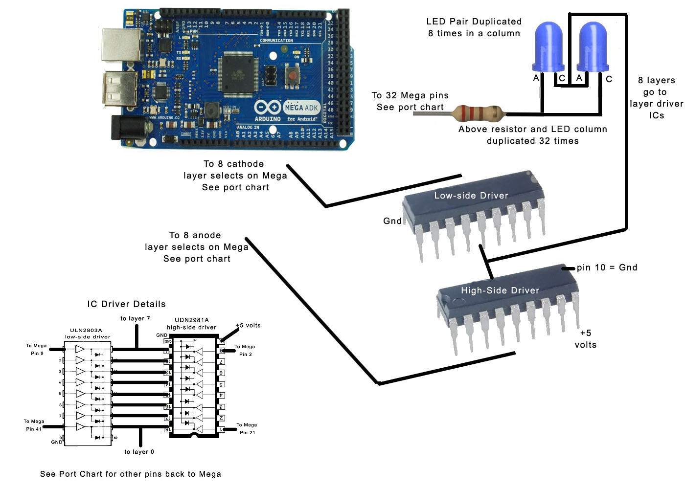
All three of my cube projects using the Mega are done without shift registers. We are relying strictly on the large number of pins available on the Mega. The trick in the case of this 8x8x8 is the somewhat whimsical approach of building our cube out of pairs of LEDs put in parallel but in opposite polarities. With voltage applied in one direction, one of the two LEDs is forward biased and lights up. With voltage applied in the other direction, the other LED is forward biased and it lights. Our refresh routine takes turns lighting up one and then the other. It happens fast enough that we see both on at the same time, if they are both programmed on.
With this approach, we only need to bring 32 columns of LEDs down to the main board, so controlling and powering a 8x8x8 cube can be done without any shift registers, directly from the Mega digital pins.
We only light up one layer at a time and even then, only half of the LEDs in that layer. But with 32 LEDs on at once, we need a transistor to handle the current. So we need 8 PNP transistors to pull our layers high when we want to light the LEDs whose cathodes go down to the main board. We also need 8 NPN transistors to pull our layers low when we want to light the LEDs whose anodes go down to the main board. My original concept as shown above would actually use 16 transistors. But it would also require pull up and pull down resistors and base current limiting resistors, so I opted to use an octal NPN IC with all that build in, and a octal PNP high side driver, again with all the resistors already built in. I also decided, in order avoid timing issues and avoid the need for inverters, to simply drive the two octal drivers each from separate digital pins on the Mega. It raises the total digital pin count to 48, but keeps the component count on the main board very low. (2 DIP ICs and 32 resistors)
We potentially have 32 LED’s on at the same time. To keep the current below Mega’s max current limit, we run the returns to the board through 220 ohm resistors, This limits LED current to 6 ma x 32 = 192 ma., just below the Mega’s 200 ma max. (If your wondering, the LEDs have a forward drop of about 3 volts and our driver transistors have a forward drop of 0.7 volts, so from our 5 volt supply, we get 1.3 volts/220 ohms = 6 ma per LED.)
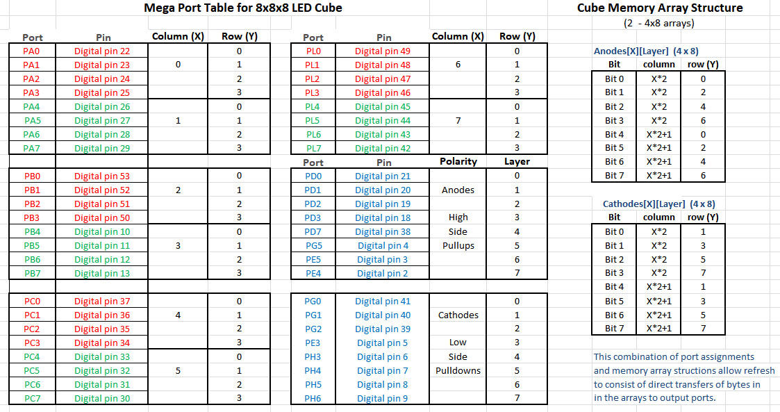
Refresh requires 16 steps – 8 for 8 layers where cathodes go to the main board, and 8 more for where anodes go to the main board. We turn on LEDs for each of these steps for 500 µsec., so our refresh cycle takes about 8 msecs, plus a little time for loading up data - configure 32 pins for each of those 16 steps. However, we are using a super efficient data load, first because we are using direct port access instead of digitalWrite, but also, because we have set up the combination of memory array and port assignment so that we accomplish each of those 16 transfers by simply storing four bytes from memory directly into the digital output ports. This approach turned out to be so efficient that I couldn't measure the time it takes. So our refresh takes just a tiny bit more than 8 ms. We set our refresh rate at 80 Hz, so refresh occurs every 12.5 msec. That means our Mega spends 2/3 of its time refreshing the cube and 1/3 of its time running in the main loop.
One other thing to note about our layer drivers and refresh routine is that we have the outputs of both our high-side and low-side drivers connected directly to the layers and each other. We need to make sure they are never on at the same time as that essentially puts a short across our Mega's 5 volt power supply. So the refresh routines not only doesn't turn them on at the same time, but adds a 3 microsecond "settling time" between layers to insure we don't get any unwanted transient currents running around in our cube.
So above we have described the concept. How does it work in reality? Well I built the cube and it works as described. Construction I think was actually slightly easier that a conventional 8x8x8 cube. (Though lead forming and soldering together 512 LEDs is never really easy.)
There are a couple of things I learned along the way. If you decide to build this cube, you might consider doing a couple of things differently than I did. LEDs in this cube are 0.6 inches apart. This 0.6 inch pitch is what I used for all three cubes. I was very happy with it on both 5x5x5 cubes, but found it somewhat difficult to see completely through this 8x8x8. You might consider using 3 mm LEDs instead of the 5 mm ones I used. Or use 5mm LEDs with 2 inch leads and increase the pitch to 0.8 inches or even 1 inch. You also might want to modify how I soldered the LEDs together so you don't have to solder right up against the base of the LED package. I found several LEDs that were damaged by heat and had to be replaced. Finally, test the heck out of everything during construction. Make sure you find and replace any defective LEDs before final construction of the cube. That's because a bad LED in this design is not just a dead LED. It turns out that the current that was suppose to go through that LED finds an alternative path through a maze of reverse biased pairs. The open LED is replaced by a bunch of "half-on" LEDs that were suppose to be off. It works great when all the LEDs work properly, but even one defective LED will make its presence known.
ConstructionI built this cube by building 8 vertical panels each 8x8 LEDs. To build a panel, the first step is to lead form and assemble 32 opposing pairs of LEDs.
The anode (longest lead) is the one sticking straight up. The cathode (shorter lead) of the other LED is soldered to the vertical anode. Then the cathode of the first LED is soldered to the anode of the second LED. Building these pairs is facilitated by drilling 2 holes in a piece of wood exactly 0.6 inches apart. The holes need to fit the LEDs fairly snugly so that they stay in place.
When you have 32 pairs, you are ready to construct a panel. The process begins with constructing four vertical columns from 8 pairs.
I used BlueTack to hold the LEDs in place until they could be soldered. I started by making clear makings in the BlueTack every 0.6 inches. This isn't a perfect process - after completing a column, you need to clean it up, meaning get it as vertically aligned as possible, and make sure all the leads coming out the side are aligned rotationally; also that the leads are horizontal and 0.6 inches apart.
Next, when you have 4 columns completed, they need to be tested. This is an important step. Fixing a problem as this stage is very easy. It gets harder and harder to fix, if you find a problem later on in construction.
I didn't do anything fancy for testing. The Uno in the background was a source for 5 volts, nothing else. A 330 ohm resistor, sitting on the proto board, limits the current. I checked each LED to make sure it lights, first with voltage in one polarity to test half the LEDs and then with reversed polarity to test the other half LEDs. If both LEDs in a pair light up, one is the wrong polarity. If neither light up, one probably has a short across it.
Once we have 4 good columns, it is time to solder them together into a panel. For that I used the same strip of BlueTack to hold two columns together, 0.6 inches apart, lining up the 8 horizontal leads and soldering them together. The horizontal leads won't all line up perfectly initially. Get a couple lined up and solder them, then line up two more and solder them,, etc. Eventually you will have all eight soldered together. Make sure the panel is flat. Make sure it is square. Make sure it is straight. Then do the same and add another column. When you have 4 columns soldered together this way, you have a finished panel.
Congratulations. Now build seven more! At this point, you are ready to begin final assembly. I built my cube on the main board, but first the board needs to be prepared by installing the other components.
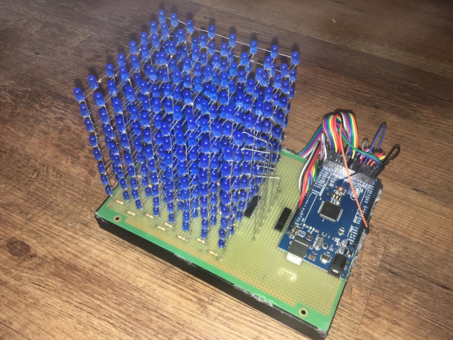
Above you can see the two IC drivers and 32 resistors mounted on the main board. The resistors are mounted 0.6 inches apart in both directions. It doesn't quite look that way in this picture for two reasons. First, I have all the resistors going from their respective column back toward the center of the cube. I did it to keep the area near the ICs from getting congested, but it probably wasn't necessary. I mounted the ICs first and, with hindsight, located them too close to the cube. There is no reason why they couldn't have been an inch lower. You can see clearly that one resistor had to be mounted out of place, because it would have been on top of the IC.
The resistors at the top of this picture are soldered in place and trimmed, but aren't connected to anything yet. The two IC are shown in the middle of the picture. The high-side driver is at the top and I used a black marker to label it A for anodes and marked pin 1 with a 1. Below it is the low-side NPN driver marked with a C for cathodes. It's pin 1 is also labeled with a 1. The two ICs are mounted this way so that their outputs face each other. This is because the output of both are tied to the layers. I have connected them to each other and spread them out a little, so that the layer returns from the cube can come down and attach to them from the other side. The connections are made with tinned copper wire. You can also see where a tinned copper wire from each IC has connected the ground pin of the IC to a ground rail on the board.
At this point, we are ready to attach 50 jumper wires to the back of the board. There are 32 going to the resistors, 8 to the inputs of the high-side driver, 8 to the inputs of the low-side driver, 1 ground wire, and 1 +5 volt wire that attaches to pin 9 of the high-side driver, its source voltage pin. These wires are all 30 cm. long and are soldered directly to their appropriate spot on the backside of the board. The other end goes around the side of the board and connects with a male jumper pin to a pin on the Mega. You can install the Mega at this point as well with some form of stand off. I actually used a couple of small squares of plastic and a little hot glue to mount the Mega myself.
We are ready to install panels. Installing a panel involves pushing the four vertical column leads through the board, leveling the layer, and then soldering the four leads to their corresponding resistor on the back side.
Each panel needs to be tested once it's installed and before the next panel is installed. That way, if there is any issue (cold solder joint, dead LED, etc.), it can be fixed before it winds up in the middle of the cube. Before we can test the first panel, however, we need to connect the layers to the board. This is accomplished by attaching a straight piece of tinned copper wire to the layer and then bringing down to one of the 8 IC outputs. And don't forget the ground and +5 connections to the Mega. The +5 goes to pin 9 on the high-side driver.
Layer 7 (the top layer) attaches to pin 18 (first channel) of the low side driver and to pin 11 (eighth channel) of the high-side driver. Layer 0 (the lowest layer) to pin 11 of the low-side driver and pin 18 of the high-side driver.
We also at this point need to attach all wires to the Mega. The table below shows what pin on the Mega is attached to each resistor. These are the connections in Red and Green. The connections to the high and low side drivers are shown in blue. They each connect to the IC directly across from their corresponding output. So for example, the low side driver output to layer 7 is pin 18 on the IC. Directly across from pin 18 is pin 1 on the IC, so the wire from pin 1 on the low-side driver attaches to pin 9 on the Mega per the chart below.
At this point, we can now test the panel. The program to test panels is included in the software. You will need to tell it which panel you are testing at the top of the sketch. The one being test in the picture is panel 0.
Once you have tested the installed panel, you can then install the next one. You have not yet installed the horizontal runners that connect the panels together for each additional layer, so you will need to put a temporary jumper between the panel you are testing and panel 0 for each layer. ( I just used one jumper and tested each layer separately, moving the one jumper from layer to layer.)
Once you have all panels installed and tested, you are ready to connect the layers. This is accomplished by running a piece of straight tinned copper wire between the panels at each layer.
Start connecting layers at the top. And be sure to measure your 0.6 inch spacing as you connect that top layer. Once you have connected the layers, your cube is complete, and you should be able to run the main show.
SoftwareWe have already talked a little bit about software. The timed refresh interrupt routine is the heart of any cube software. I designed this one to be very simple and efficient. That required using two different memory arrays to store the status of each LED in the cube. So one stores the status of the LEDs whose anodes come down to the board and the other stores the status of the LEDs whose cathodes come down to the main board. These two arrays store the x and z values by their position in the array, and they store the y value as the bits at that location. A bit set to 1 says that LED is on, and a bit set to 0 says that LED is off. Again, all this is very efficient, but it can be very confusing to try and figure out how to set a particular LED in the cube as on or off. So the other key to our basic support software is an ledOn(x, y, z) and an led0ff(x, y, z). These subroutines do all the hard work of figuring out which bit in those two arrays needs to be changed to turn a specific LED on or off.
So with subroutines to turn any particular LED on or off, and a refresh routine that continually lights and updates the cube to match the content of our arrays, it is fairly easy to create various animations and special effects. Our main sketch, called the Show, is several minutes of animations created to demonstrate the cube's performance.
There is one other topic to discuss under software. Most of the animations in the Show are straight forward turn on and then turn off patterns of LEDs. Some use a little math to control those patterns. But there a few animations in the Show of another type. These are based on an object class called a sprite. The sprite class defines an object in the cube. A object in the sprite can be moved around, bounced, rotated, etc. It allows the fairly easy creation of some animations that would be very difficult to create without object based code.


_wzec989qrF.jpg?auto=compress%2Cformat&w=48&h=48&fit=fill&bg=ffffff)


Comments
Please log in or sign up to comment.