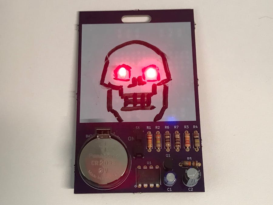
Recently, I was trying to learn KiCAD for PCB layout. I came across this very useful tutorial KiCAD by Digi-Key. It is not only a tutorial of PCB layout, but also an example of the PCB fabrication flow. So I decided to follow the tutorial and make a digital badge for myself. On the front silk screen, I draw a terminator symbol with a marker for fun. You can draw whatever you like.
I will not elaborate the whole process here, cause the tutorial is instructed so well. But I do have some comments just in case it might be useful for you.
1) The 2N3904 footprint is too small for hand soldering. I didn't succeed until I wasted two PCB boards (luckily OSHpark requests minimum 3 boards per order). I would suggest you using a larger footprint for your own convenience.
2) The soldering pads can be larger than the tutorial uses. This will also ease the hand soldering
3) Before soldering, use some alcohol to rub the soldering pad. I think there is some residuals that makes solder hard to attach.
Finally, it is show time. Let have a look at the video.


_4YUDWziWQ8.png?auto=compress%2Cformat&w=48&h=48&fit=fill&bg=ffffff)


Comments
Please log in or sign up to comment.