Source: https://www.pcbway.com/blog/technology/Low_Noise_Adjustable_Linear_AC_DC_Power_Supply.html
[1] LM317 Datasheet: http://www.ti.com/lit/ds/slvs044x/slvs044x.pdf
[2] LM337 Datasheet: http://www.ti.com/lit/ds/symlink/lm137.pdf
[3]: Schematic Symbol and PCB Footprint for LM317: https://componentsearchengine.com/part.php?partID=248007
[4]: Schematic Symbol and PCB Footprint for LM337: https://componentsearchengine.com/part.php?partID=290650
[5]: Altium Plugin: https://www.samacsys.com/altium-designer-library-instructions
Features:AC – DC Conversion
Double output voltages (Positive – Ground – Negative)
Adjustable positive and negative rails
Just a Single-Output AC transformer
Output noise (20MHz-BWL, no load): Around 1.12mVpp
Low noise and stable outputs (ideal to power Opamps)
Output Voltage: +/-1.25V to +/-25V
Maximum output current: 300mA to 500mA
Cheap and easy to solder (all component packages are DIP)
A double output low noise power supply is an essential tool for any electronics enthusiast. There are many circumstances that a double-output power supply is necessary such as designing pre-amplifiers and powering OPAMPs. In this article, we are going to build a linear power supply that a user can adjust its positive and negative rails independently. Moreover, just an ordinary single-output AC transformer is used at the input.
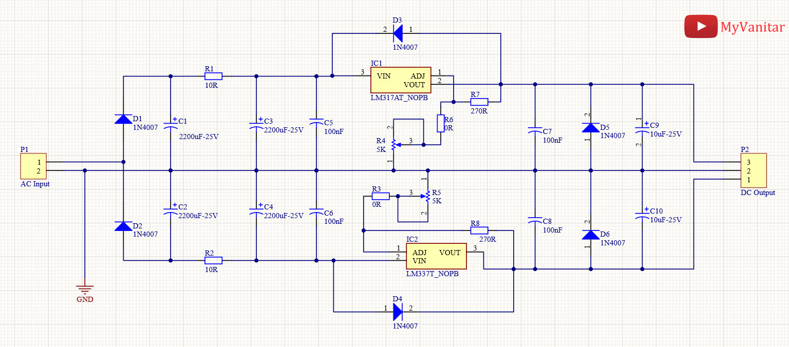
[1] Circuit AnalysisFigure 1 shows the schematic diagram of the device. D1 and D2 are rectifier diodes. C1 and C2 build the first noise reduction filter stage.
R1, R2, C1, C2, C3, C4, C5, and C6 build a low pass RC filter which reduces noise from both positive and negative rails. The behavior of this filter can be examined both in theory and practice. An oscilloscope with a bode plot feature can perform these measurements, such as a Siglent SDS1104X-E.
IC1 [1] and IC2 [2] are the main regulation components of this circuit. According to the IC1 (LM317) datasheet: “The LM317 device is an adjustable three-terminal positive-voltage regulator capable of supplying more than 1.5 A over an output-voltage range of 1.25 V to 37 V. It requires only two external resistors to set the output voltage. The device features a typical line regulation of 0.01% and a typical load regulation of 0.1%. It includes current limiting, thermal overload protection, and safe operating area protection. Overload protection remains functional even if the ADJUST terminal is disconnected”.
As it is clear, this regulator introduces good line and load regulation figures, therefore we can expect to get a stable output rail. This is identical to the IC2 (LM337). The only difference is that this chip is used to regulate the negative voltages.
D3 and D4 are used for protection. The diodes provide a low-impedance discharge path to prevent the capacitors (C9 and C10) from discharging into the output of the regulators.
R4 and R5 are used to adjust the output voltages. C7, C8, C9, and C10 are used to filter the remained output noises.
[2] PCB LayoutFigure 2 shows the PCB layout of the circuit. It is designed on a single-layer PCB board and all component packages are DIP. Pretty easy for everyone to solder the component and start using the device.
I used the SamacSys component libraries for IC1 [3] and IC2 [4]. These libraries are free and more importantly follow industrial IPC footprint standards. I use Altium, so I directly installed the libraries using the Altium plugin [5]. Figure 3 shows the selected components. Similar plugins can be used for KiCad and other CAD software.
Figure 4 shows a 3D view of the PCB board.
Figure 5 shows the assembled board. I decided to use a 220V to 12V transformer to get maximum +/-12V at the output. Figure 6 shows the required wiring.
By turning the R4 and R5 multiturn potentiometers, you can adjust the voltages on the positive and negative rails independently. Figure 7 shows an example, where I have adjusted the output at +/-9V.
Now it’s time to measure the output noise. I used the Siglent SDS1104X-E oscilloscope that introduces 500uV/div sensitivity at the input which makes it ideal for such measurements. I put the channel-one on 1X, AC coupling, 20MHz bandwidth limit, then set the acquisition mode on peak-detect. Then I removed the ground lead and used a probe ground-spring. Note that this measurement is under no output load. Figure 8 shows the oscilloscope screen and the test result. The Vpp figure of the noise is around 1.12mV. Please note that increasing the output current will increase the noise/ripple level. This is a true story for all power supplies.
The power rate of R1 and R2 resistors define the output current. So I selected 3W resistors. Also, if you intend to draw high currents or the voltage difference between the input and output of the regulator is high, don’t forget to install suitable heatsinks on IC1 and IC2. You can expect to get 500mA (max) by using 3W resistors. If you use 2W resistors, this value naturally decreases to somewhere 300mA (max).
[4] MaterialsFigure 9 shows the bill of materials.


Comments
Please log in or sign up to comment.