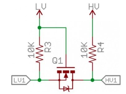
In digital electronics, a level shifting circuit, called a logic-level shifter or a voltage level translator, is a circuit used to translate signals from one logic level or voltage domain to a level. This is needed to meet the compatibility between ICs with different voltage requirements, such as TTL and CMOS. The level shifter is used to bridge processors, logic circuits, sensors, and other circuits. The lowest three-level logic commonly used is 1.8 V, 3.3 V, and 5 V.
Bi-directionallogic converterOne circuit commonly used is the bi-directional logic level converter circuit that uses single-channel NMOS. This circuit can change the logic level with a higher voltage to a lower voltage and vice versa.
Non-invertingop-amp level shifter
In addition to the different voltage levels for logic circuits, there are often voltage differences for signals obtained from sensors with voltages on the microprocessor. A circuit is needed that can convert positive-negative voltage signals into voltages that match the ADC single supply range. For this reason, a non-inverting op-amp level shifter is used.
The example circuit above converts the +- 5 V signal from a sensor into a signal with a voltage of 0- 3.3 V so that it can be processed by the ADC on the microprocessor. The equation for amplifying the input voltage and offset voltage is
By taking the values 𝑅1 = 𝑅3 and 𝑅2 = 𝑅4 then
To convert a 10 Vpp signal to a 3.3 v signal an A of 1/3 is required. A value of 𝑅4 of 33K and 𝑅1 of 100K can be selected. Furthermore, a positive offset is needed so that the center of the signal is at a voltage of 1.6 V. With the previous resistor value, the gain offset is 1 so that the offset voltage used is 1.6 V.
The thing to be done- Verify the HV pin output on the bi-directional logic converter
- Verify the LV pin output on the bi-directional logic converter
- Verifies the non-inverting op-amp level-shifter output
- Modify the non-inverting op-amp Level-shifter
Make a circuit like Figure 1 on the breadboard. Then do the verification by measure the LV pin voltage and providing input variations on the HV pin. The following results are obtained:
From the above table, it can be concluded that if the input voltage is below 1.6 V, the output voltage will be close to 0 V. If the voltage is handled 1.6 V, the output will be close to 5 V. If the input voltage is 1.6 V, the output can sometimes approach 0 V or 5 V. Depending how close is the 1.6 V value to 0 V or 5 V because the value does not fit 1.6 V because there is noise which makes it inappropriate 1.6 V.
Verify the LV pin output on the bi-directional logic converterMake a circuit like Figure 1 on the breadboard. Then do the verification by measure the HV pin voltage and providing input variations on the LV pin. The following results are obtained:
From the above table, it can be concluded that if the input voltage is below 2.5 V, the output voltage will be close to 0 V. If the voltage is handled 2.5 V, the output will be close to 3.3 V. If the input voltage is 2.5 V, the output can sometimes approach 0 V or 3.3 V. Depending how close is the value of 2.5 V to 0 V or 3.3 V because the value is not right 2.5 V because there is noise which makes it inappropriate 2.5 V.
Verifies the non-inverting op-amp level-shifter outputCreate a circuit on a breadboard like Figure 2. Then verify the circuit by providing variations in the input voltage, the following results are obtained:
From the above experimental results, it was concluded that the output of a non-inverting op-amp circuit is continuously different from the discrete bi-directional circuit. From the table it can be seen that the value reaches saturation up to 2.05 V because this transistor may not be of good quality. The resistor value in the circuit has been checked and it's not too far off. The op-amp saturation input value has been made larger but only reaches 2.35 V as shown.
Modify the non-inverting op-amp Level-shifterA circuit design is needed to convert the + 2.1 V signal to the 0 - 5 V signal.
To get the circuit with these characteristics, it is necessary to make a modification in Figure 2. Based on the formula in the non-inverting circuit op-amp level shifter, the resistance value and reference voltage are selected as follows:R2 = R4 = 120K ΩVref = 2.5 VV + = 6VV- = -3 V
In the Voltage Shifter Circuit (High-Level Shifters) it can be observed that high voltage and low voltage outputs in the bi-directional logic level converter circuit produce discrete signals on or off. At the output level of the non-inverting op-amp level shifter, a continuous output is obtained.


Comments
Please log in or sign up to comment.