


Hardware components | ||||||
 |
| × | 1 | |||
Software apps and online services | ||||||
| ||||||
A demo to illustrate:
(1) Creating/packaging custom IP for use in the programmable logic (PL) of a SoC design
(2) Executing memory-mapped register write/read operations from the SoC processor system (PS)
I use a MiniZed board here, which has a Zynq FPGA, but these concepts apply to any SoC design. Even though these are relatively basic concepts, there are a lot of housekeeping steps and settings. I use Vivado/Vitis 2020.2, but the steps should be very similar for earlier versions of Vivado/SDK as well.
Use the outline below to skip around as needed; bold steps highlight the key design items.
1B. Outline1. Overview
2. Vivado - SoC Project Setup
2A. New Project Creation
2B. Block Design Setup
2C. Custom IP Setup: specify the AXI interface and memory-mapped registers
3. Vivado - IP Editor Project
3A. Verilog Adder: specification for an adder module
3B. Packaging the IP
4. Vivado - SoC Project Implementation: using the adder in the base project
5. Vitis - Application Project Setup
5A. Initial Setup
5B. Creating a Random Number Addition Application: C code and explanation
5C. Running the application: seeing results over UART
6. Analysis & Conclusion
2. Vivado - SoC Project Setup2A. New Project Creation1) Open Vivado. Click create a new project, give it a name (e.g. ps_pl_demo), and click next.
2) RTL Project -> Do not specify sources, click next.
3) Choose your board* from the Boards tab, click next, then click finish.
* For first-time setup, you may need board definition files for your dev kit. Minized's are here under "Technical Documents" -> "Board Definition Files". If needed, download and unzip that file. The top-level directory for the board (minized/ in this case) must be copied your Vivado installation directory (e.g. /home/user/Applications/Xilinx/Vivado/2020.2/data/boards/board_files/).
2B. Block Design Setup1) Once finished with Vivado's new project GUI, you'll be taken to the standard Project Summary page. Click Create Block Design from the Flow Navigator pane.
2) A popup appears asking for a block design name: the default name is fine.
3) Now the 'Diagram' pane appears. Click the '+' button and in the popup menu, double-click 'ZYNQ7 Processing System'. A block for the PS appears:
1) Now, from the top menu bar, click "Tools -> Create and Package New IP". Click next, then "Create a new AXI4 peripheral" on the following screen and hit next again:
2) On the following screen, give the IP a name. In this demo I'll show a simple adder, so my IP name is axi4l_adder. Note the directory location in the bottom field, we'll navigate there shortly:
3) Click next, and the following page appears:
The default settings are fine for this demo. They will generate four, 32-bit registers in the PL. 4*32 = 128 bits, so the PS will be able to address 16 bytes of memory-mapped register space in this PL module.
4) Click next and scroll to the section with "Next steps". Select "Edit IP" and click Finish. A new Vivado project will open.
3. Vivado - IP Editor Project3A. Verilog Adder1) This new Vivado project is where we will edit the axi4l_adder IP. The default pane should have all of the previous information:
And the Design Sources pane should contain some auto-generated Verilog:
2) Double-click axi4l_adder_v1_0_S00_AXI.v and Vivado will open a new tab with the HDL source. The module I/O has all of the signals for the AXI4-Lite slave interface; don't touch. The four expected registers are below the I/O region:
Let's define the adder's expected behavior:
- slv_reg0: addition term 1, written by the PS
- slv_reg1: addition term 2, written by the PS
- slv_reg2: sum of terms 1 and 2, calculated by the PL
- slv_reg3: carry from the addition, calculated by the PL
So we define their permissions:
Back in the Verilog file, below the reg declarations, there are automatically generated processes which facilitate the AXI signaling, as well as the register write/read management. We need to do a few things: (1) prevent the PS from writing at slv_reg2 and slv_reg3, (2) calculate the sum and carry in PL, (3) write them to slv_reg2 and slv_reg3.
3) To prevent the PS from writing at forbidden registers, we must update the dedicated process which manages memory-mapped register writes. Search for the comment "// Implement memory mapped register select and write logic generation" around line 210. Comment out the slv_reg2 and slv_reg3 assignments, or remove them altogether:
Now the PL may manage these registers instead.
4) Return to line 115 or so. Provision for an addition reg type called sum. Its size will be one bit larger than the slv_reg* signals, to accommodate the carry bit.
reg [C_S_AXI_DATA_WIDTH-0:0] sum;5) Now, navigate to the bottom of the file ("//Add user logic here"). Create a process which calculates the sum of reg0 and reg1, then writes to slv_reg2&3.
// Add user logic here
    always @( posedge S_AXI_ACLK )
	begin
	  if ( S_AXI_ARESETN == 1'b0 )
	    begin
	      sum <= 0;
	      slv_reg2 <= 0;
	      slv_reg3 <= 0;
	    end
	  else begin
	    sum         <= slv_reg0 + slv_reg1;
	    slv_reg2    <= sum[$high(sum)-1:0]; // lower 32 bits
	    slv_reg3[0] <= sum[$high(sum)];     // top carry bit
      end
    end
// User logic ends
Hit Ctrl+E after pasting this code. In the Source File Properties pane, change Type: Verilog to Type: SystemVerilog. This is necessary for using system calls such as $high().
Save the file and let's wrap up the IP.
3B. Packaging the IP1) Return to the "Package IP" tab. The check mark has been removed from the "File Groups" section since we modified the Verilog source. Hit "Merge changes":
2) Now under the "Review" section, click "Re-package":
3) Now a popup should appear; close the IP project and return to the SoC project.
4. Vivado - SoC Project Implementation1) Back in the SoC project, we can use the new adder IP:
Search for axi4l_adder, double-click the search result, then hit the green banner text for "Run Connection Automation" and use the default settings. This step makes the connection from the Zynq M_AXI_GP0 to the adder IP via the AXI interconnect block.
Then click "Run block automation" and use the default settings. This step is necessary for using the Zynq's UART1 interface during software development.
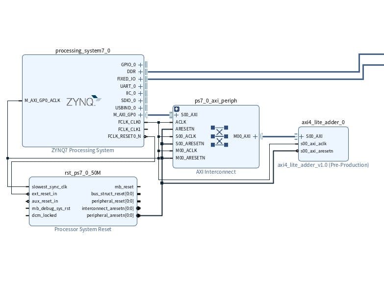
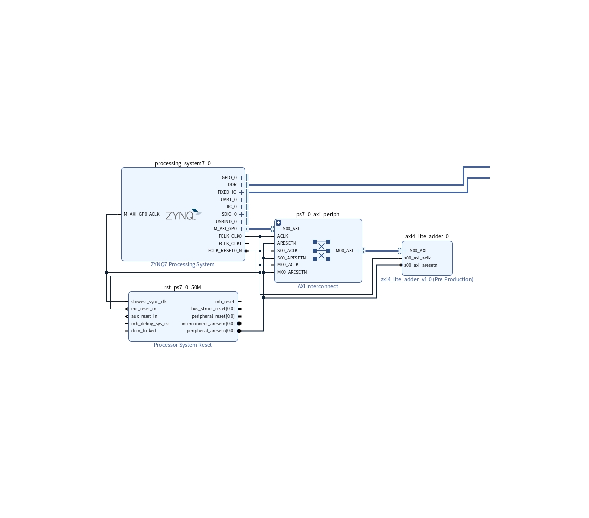
2) The block design should populate with an AXI interconnect and reset manager:
M_AXI_GP0 of the PS should be wired to the AXI interconnect, and M00_AXI of the interconnect should be wired to the AXI4L adder IP. If you don't see M_AXI_GP0 on the PS block, you'll need to double-click the block and select "M AXI GP0 interface" on the PS-PL configuration tab, under the dropdown for "AXI Non Secure Enablement".
3) In the Address Editor tab ("Window" -> "Address Editor"), you should see the adder IP listed:
4) Hit the F6 key to validate the block design.
5) In the Sources pane, under Design Sources, right-click the.bd file and select "Create HDL wrapper" -> "Let Vivado manage and auto-update."
6) Hit the "Generate Bitstream" button (or "Flow" -> "Generate Bitstream") to let synthesis and implementation run. Vivado constraints aren't required since this is a simple PS project. Under design runs, you'll see the adder IP under OOC runs:
7) Once bitstream generation completes, close the popup and navigate to "File" -> "Export" -> "Export Hardware". Hit next on the welcome screen. On the following screen, select "Include Bitstream." Give the hardware specification a name and save it in the SoC project directory. The output is a XSA file for use in Vitis below.
5. Vitis - Application Project5A. Initial Setup1) [Optional] Create a Vitis workspace folder (e.g. within the SoC project folder).
2) From Vivado, hit "Tools" -> "Launch Vitis IDE"
3) Vitis may either load to a welcome screen or it may begin inside a previous workspace. If it begins inside a previous workspace, hit "File" -> "Switch Workspace" and point to the new directory [also optional].
4) Click Create Application Project ("File" -> "New" -> "Application Project"). Hit Next at the welcome page.
5) On the platform page, click the tab for "Create a new platform from hardware (XSA). Now Browse to select the XSA file exported from Vivado.
6) We'll be adding together some random numbers. Create a new application project called rn_addition and hit Next.
7) On the next page "Domain", the default settings are fine.
8) On the "Templates" page, select the Hello World template and hit Finish.
9) Now in the Vitis explorer, select the Application Project settings entry (rn_addition.prj) and click "Navigate to BSP settings",
10) Now click "Modify BSP Settings":
11) Under the "Standalone" tab, set stdout to ps7_uart1. This enables software prints using the Zynq's UART. Click Ok and return to the Application Project settings tab.
12) On the Application Project settings tab, click Hardware Specification:
13) In the resulting tab, the AXI4L adder should be in the address map:
1) Now we can do something useful. In the Vitis explorer pane, expand src. Rename helloworld.c as rn_main.c and double-click to edit.
Replace the helloworld code with the following:
// J. Abate '21
#include <stdio.h>
#include <stdlib.h> // for random number function
#include <unistd.h> // for sleep function
#include "platform.h"
#include "xil_printf.h"
#include "xil_io.h"

#define ADDER_b 0x43C00000
#define REG_0_o 0x0
#define REG_1_o 0x4
#define REG_2_o 0x8
#define REG_3_o 0xC

int main()
{
    init_platform();
    print("\nps7_uart_1 @ 115200 baud\n\n\r");

    // random numbers; bottom and top of range
    u32 rn_lo = 0x40000000, rn_hi = 0xBFFFFFFF;

    // register data
    u16 test_count = 1;
    u32 slv_reg0_wdata = 0xFFFFFFFF;
    u32 slv_reg0_rdata;
    u32 slv_reg1_wdata = 0x1;
    u32 slv_reg1_rdata;
    u32 slv_reg2_rdata;
    u8  slv_reg3_rdata;

    while(1)
    {
    	xil_printf("test #%d\n\r", test_count);

    	// Write then read slv_reg0
    	Xil_Out32(ADDER_b + REG_0_o, slv_reg0_wdata);
    	slv_reg0_rdata = Xil_In32(ADDER_b + REG_0_o);
    	xil_printf("slv_reg0 [w]|[r] = 0x%08X | 0x%08X (%u) \n\r", slv_reg0_wdata, slv_reg0_rdata, slv_reg0_rdata);

    	// Write then read slv_reg1
    	Xil_Out32(ADDER_b + REG_1_o, slv_reg1_wdata);
    	slv_reg1_rdata = Xil_In32(ADDER_b + REG_1_o);
    	xil_printf("slv_reg1 [w]|[r] = 0x%08X | 0x%08X (%u) \n\r", slv_reg1_wdata, slv_reg1_rdata, slv_reg1_rdata);

    	// Read slv_reg2&3
    	slv_reg2_rdata = Xil_In32(ADDER_b + REG_2_o);
    	slv_reg3_rdata = Xil_In8(ADDER_b + REG_3_o);
    	xil_printf("sum [r] | c [r]  = 0x%08X | 0x%01X        (%u) \n\n\r", slv_reg2_rdata, slv_reg3_rdata, slv_reg2_rdata);

    	// update terms for next iteration and increment the test count
    	slv_reg0_wdata = ( rand() % (rn_hi - rn_lo + 1) ) + rn_lo;
    	slv_reg1_wdata = ( rand() % (rn_hi - rn_lo + 1) ) + rn_lo;
        test_count += 1;

    	sleep(10);
    }


    cleanup_platform();
    return 0;
}
2) Code explanation. I included the following files:
- stdlib.h for the rand() function
- unistd.h for the sleep() function
- xil_io.h for the memory-mapped register R/W functions Xil_In() and Xil_Out()
Then I define the memory addresses to use. The Vivado address editor and the Vitis address map reserve 64KB of addresses for the adder IP at base 0x43C00000 (offsets 0x0 to 0xFFFF).
However, recall that the adder IP only has four, 32-bit registers, for a total of 16 bytes (0x0 to 0xF):
- slv_reg0 (offsets 0x0 to 0x3): write the 1st addition term here
- slv_reg1 (offsets 0x4 to 0x7): write the 2nd addition term here
- slv_reg2 (offsets 0x8 to 0xB): read the sum here
- slv_reg3 (offsets 0xC to 0xF): read the carry bit here
Inside the while(1) loop, the Xil_Out() and Xil_In() statements manage the writes/reads at each register.
5C. Running the application1) Back in the Vitis explorer pane, collapse all of the expanded entries. Highlight both the platform project and the application project, then right-click and hit "Build Projects". Once the build is done, hit the dropdown next to the Bug button and click Debug Configurations.
2) In the resulting popup, double-click "System Project Debug" and move to the Target Setup tab. Ensure "Program FPGA" is selected, then hit Debug to close the popup.
3) Now, connect a USB cable from the computer to the USB/JTAG/UART port of the MiniZed. Open a serial session with the MiniZed UART at 115200 baud:
4) Back in Vitis, hit the Run button:
5) In the serial session, you should see prints similar to this:
Each test shows the following:
- The test ID#
- The terms written to slv_reg0 and slv_reg1, to the right of each equal sign
- The terms read from slv_reg0 and slv_reg1, to the right of each pipe sign (unsigned in parentheses).
- The sum and carry results read back from slv_reg2 and slv_reg3 (unsigned sum in parentheses).
The first test is hard-coded to show the successful read from the carry bit register. Subsequent tests are psuedo-random.
6. Analysis & ConclusionThis demo shows PS-PL data transfer over an AXI4-Lite interface by using Xil_In() and Xil_Out() from the PS. Any time the PS issues a Xil_Out() to write a new term at slv_reg0 or slv_reg1, the PL always updates the sum of the slv_reg0 and slv_reg1 terms.
On the first clock cycle after either term is written by the PS, the PL calculates the new sum. On the second clock cycle, it updates slv_reg3 with the sum result and slv_reg4 with the carry result. That latency is small (two periods of FCLK_0 = 40 ns), compared to time which elapses between the Xil_Out32() to slv_reg1 and the Xil_In32() of slv_reg2. In that sense, this demo assumes the PL always has valid results by the time the PS reads slv_reg2 and slv_reg3.


Comments
Please log in or sign up to comment.