


Hardware components | ||||||
 |
| × | 1 | |||
Software apps and online services | ||||||
| ||||||
 |
| |||||
Dreaming digital circuit design and playing with the Arty Z7-10 board, working on various projects. Let's get acquainted with the FPGA board together by undertaking diverse projects.
"I have redesigned the Watch code from https://www.hackster.io/matbi. Additionally, I have implemented the ability to count days and years. "
IP TOP (CORE)Watch IP
Our Watch IP has input signals including a 100MHz clock (clk), a reset signal, an enable signal for the module (I_run_enable), and a frequency-setting signal for the one_sec_gen (I_freq). The output signals include the seconds, minutes, hours, days, years.(o_sec, o_min, o_hour, o_day, o_year).
We generate a continuous 1-second signal using the one_sec_gen module. With a 100MHz input clock frequency, setting I_freq to 100MHz results in the generation of a 1-second signal. When the counting value reaches I_freq-1 in the one_sec_gen module, a one-cycle high signal is sent to the tick_gen module, generating the output tick.
The tick_gen module consists of tick_gen_sec, tick_gen_min, tick_gen_hour, tick_gen_day, and tick_gen_year cascaded together. For example, the output tick of tick_gen_sec is connected to the input tick of tick_gen_min.
During our analysis, we observed a delay between the counting value and the tick_gen output. Both sec and min have a 1-cycle delay, and hour has a 2-cycle delay. This delay occurs because the output tick, being a flip-flop (F/F), does not immediately transmit the tick when it is I_freq-1; instead, it is transmitted in the next cycle. Consequently, we introduced a 2-cycle delay for sec and a 1-cycle delay for min in the tick_gen module to align them with the hour.
AXI4-Lite
Here, we are using a type of AMBA system known as AXI4-Lite. Through this, we can control hardware Intellectual Property (IP), and with our Watch IP, we can provide the desired I_freq value. Additionally, we can read the values of seconds, minutes, and hours.
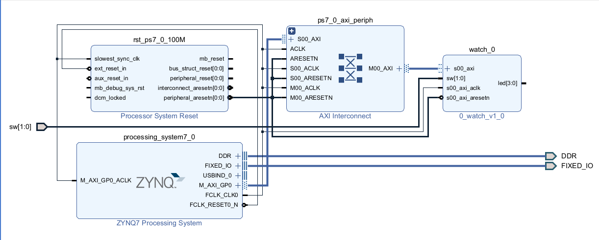
HW SYSTEM
We invoked our previously created Watch IP and ZYNQ in Vivado. The ZYNQ (PS) is configured at 100MHz, and for the Arty Z7-10 board used here, we set the UART 0 to MIO14-15 and both BANK 0, 1 I/O voltages to LVCMOS 3.3V. Afterward, we wired the circuit using auto-connection.
SWI (SoftWareInterface)
Register table is here.
RUN
Normal mode ( input freq value : 100, 000, 000)
Fast mode ( input freq value : 100, x1, 000, 000 times faster)
SUMMARY
So far, we have created our own watch using Verilog and FPGA. Developing our custom hardware IP and utilizing UART communication with the PS allowed us to control the IP, enabling us to read and write desired values. While the Watch Project may seem simple, it serves as a significant stepping stone for undertaking various projects using FPGA in the future. Additionally, through the projects we have undertaken, we had a great opportunity to explore and indirectly experience the diverse functionalities of FPGA. I believe that continuing to work with FPGA features will lead to the execution of various projects. Looking forward, we plan to leverage the capabilities of FPGA in diverse projects.
Thank you so much to read! Have a good day :)


Comments