


Hardware components | ||||||
 |
| × | 1 | |||
 |
| × | 1 | |||
 |
| × | 1 | |||
 |
| × | 1 | |||
 |
| × | 5 | |||
 |
| × | 1 | |||
 |
| × | 1 | |||
Software apps and online services | ||||||
 |
| |||||
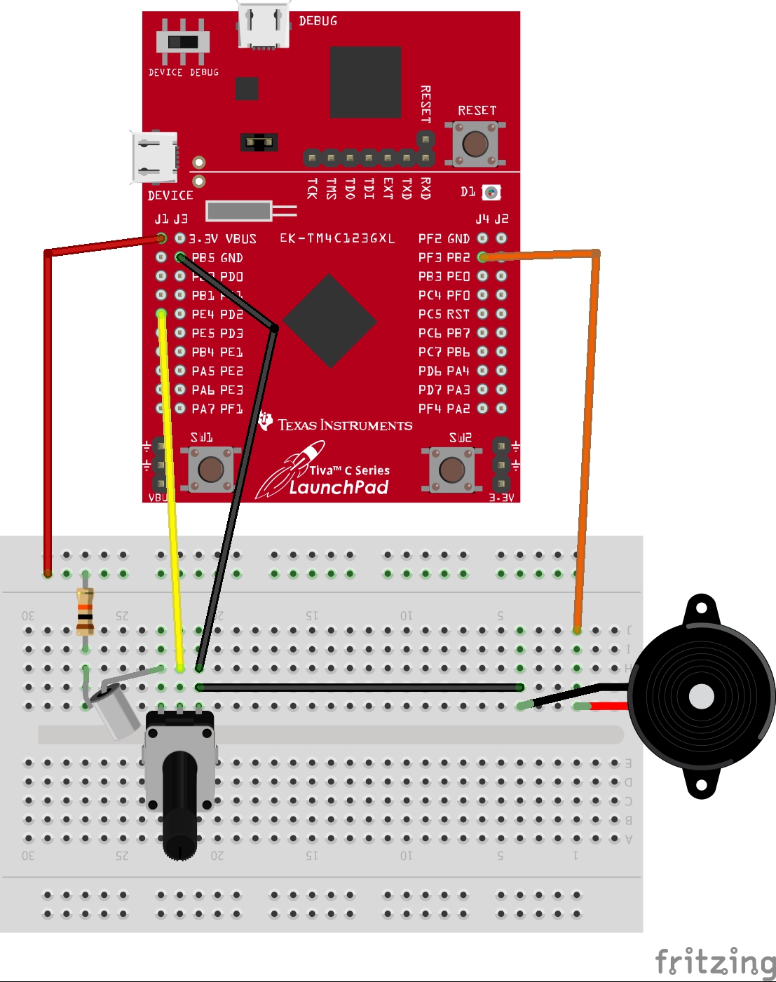
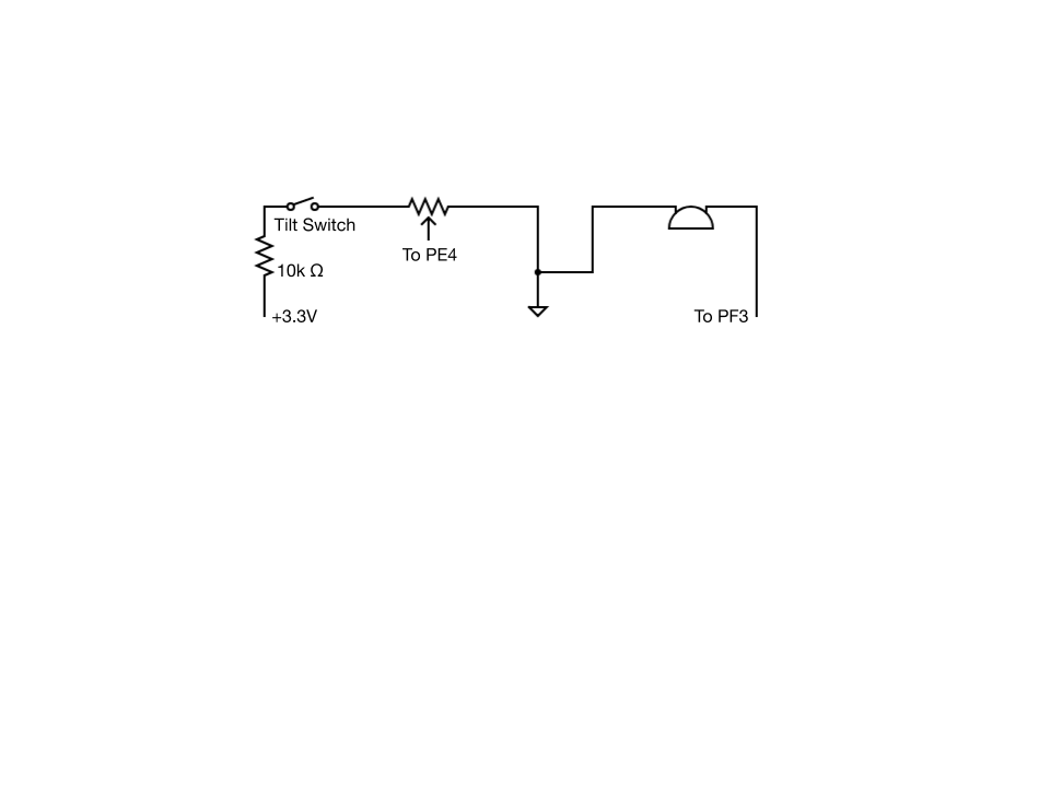
Eduardo, Emmy, Jacob, and Lisa were sitting on the couch watching an NBA game, when suddenly, they heard a phone ring. The NBA was on the other end of the line. One of the most vaunted professional basketball players, Dr. Ray Simar, had suggested that his team start singing a capella as a bonding and team strengthening exercise. Besides, such a venture would surely bring in additional revenue if it took off. Word spread, and many other players, including Lebron James and Michael Jordan, agreed, being avid music lovers themselves. It became so popular that the NBA as a whole decided to implement this idea. Consequently, they needed what essentially was a pitch pipe, but more technologically adaptable. The quartet jumped into action, developing an adjustable buzzer to suit the NBA's needs. All anyone had to do was turn the dial to select the necessary key, and everyone could live out their High School Musical dreams.
/*
 * main.c
 *
 *
 * This is the configuration we will use:
 * 		+ 	Our input pin will be PE4.
 *			Not used as a GPIO, but using its Alternate Function
 *		+	There are two ADC modules.  We will use ADC0.
 *		+	We will configure it for a sample rate of 125 kHz.
 *		+	We will start sampling via software and poll to determine when data is ready.
 *			This will be how we synchronize the CPU with ADC0.
 *
 * 	This example will follow the configuration used by Valvano in section 10.4.1 TM4C ADC details
 *
 * Date: April 21 2020
 */

#include "ADC0_registers.h"

extern void System_Clock_Init(void);
extern void ADC0_InitSWTriggerSeq3_PE4(void);
extern unsigned int ADC0_Sample_Seq3(void);

int main(void) {

        unsigned int volatile *pGPIODATA_PortE = (unsigned int *) (0x40024000 + 0x3FC);

        int sample_ADC0,i;

        System_Clock_Init();

        // Function that sets up the ADC
        ADC0_InitSWTriggerSeq3_PE4();

        // Set up the pointers to all of our registers.
        unsigned int volatile *pRCGCGPIO = (unsigned int *) (0x400FE000 + 0x608);
        unsigned int volatile *pGPIOLOCK_PortF = (unsigned int *)(0x40025000 + 0x520);
        unsigned int volatile *pGPIOCR_PortF = (unsigned int *)(0x40025000 + 0x524);
        unsigned int volatile *pGPIODIR_PortF = (unsigned int *) (0x40025000 + 0x400);
        unsigned int volatile *pGPIOAFSEL_PortF = (unsigned int *) (0x40025000 + 0x420);
        unsigned int volatile *pGPIODEN_PortF = (unsigned int *) (0x40025000 + 0x51C);
        unsigned int volatile *pGPIODATA_PortF = (unsigned int *) (0x40025000 + 0x3FC);

        // Set up Port F
        *pRCGCGPIO = *pRCGCGPIO | 0x0020;
        while ( (*pRCGCGPIO & 0x0020) == 0 ) ; // Good thing this is volatile!

        *pGPIOLOCK_PortF        = 0x4C4F434B;
        *pGPIOCR_PortF = *pGPIOCR_PortF | 0x1F;

        // SET UP PIN 3 for the speaker.
        *pGPIODIR_PortF = *pGPIODIR_PortF | 0x08;  // 0x08 looks familiar. This would SET a 1 (because of the OR) on the 3rd bit of the register. This sets Pin F3 to be an output.
        *pGPIOAFSEL_PortF = *pGPIOAFSEL_PortF & ~0x08; // No alternative functions for this pin
        *pGPIODEN_PortF = *pGPIODEN_PortF | 0x08; // Digital enable the pin

        while(1)
        {
                sample_ADC0 = ADC0_Sample_Seq3();
                float sample_voltage = (3.3/4095.0) * (float) sample_ADC0;

                //Define wait time based on voltage read
                float wait_time = sample_voltage*1000;

                //Do a square wave! (Turn on the pin, wait, turn off the pin, wait (Pin F3)
                *pGPIODATA_PortF |= 0x08;
                for (i = 1; i <= wait_time; i++){

                }

                *pGPIODATA_PortF &= ~0x08;
                for (i = 1; i <= wait_time; i++){

                }
                // Alternatively:
                // for(i = 1; i <= wait_time; i++){}
                // *GPIODATA ^= pin3;
        }
        return 0;
}
ADC0_registers.h
C/C++/*
* ADC0_registers.h
*
* Created on: Mar 28, 2016
* Author: Ray
*/
#ifndef ADC0_REGISTERS_H_
#define ADC0_REGISTERS_H_
/*
* First define the pointers to the key registers needed for configuring the PLL
*/
// pRCC2 is a pointer to the Run-Mode Clock Configuration 2 Register (DS p 260)
extern unsigned int volatile *pRCC2;
// pRIS is a pointer to the Raw Interrupt Status Register (DS p244)
extern unsigned int volatile *pRIS;
/*
* Next, define the pointers to the key registers needed for configuring
* PE4 as an analog input. Note that the use of volatile ensures that
* the compiler always carries out the memory accesses, rather than optimizing
* them out (for example, if the access is in a loop).
*/
// pRCGCGPIO is a pointer to the General-Purpose Input/Output Run Mode Clock Gating Control Register (DS p 340)
extern unsigned int volatile *pRCGCGPIO;
// pPRGPIO is a pointer to the General-Purpose Input/Output Peripheral Ready Register (DS p 406)
extern unsigned int volatile *pPRGPIO;
// pGPIODIR_PortE is a pointer to the GPIO Direction register for port E on the APB bus (DS p 663)
extern unsigned int volatile *pGPIODIR_PortE;
// pGPIOAFSEL_PortE is a pointer to the GPIO Alternate Function Select register for port E on the APB bus (DS p 672)
extern unsigned int volatile *pGPIOAFSEL_PortE;
// pGPIODEN_PortE is a pointer to the GPIO Digital Enable register for port E on the APB bus (DS p 682)
extern unsigned int volatile *pGPIODEN_PortE;
// pGPIOAMSEL_PortE is a pointer to the GPIO Analog Mode Select register for port E on the APB bus (DS p 687)
extern unsigned int volatile *pGPIOAMSEL_PortE;
/*
* Now define the memory mapped register addresses needed to configure A to D converter ADC0
*/
// pRCGCADC is a pointer to the Analog-to-Digital Converter Run Mode Clock Gating Control Register (DS p 352)
extern unsigned int volatile *pRCGCADC;
// pADCPC_ADC0 is a pointer to the ADC Peripheral Configuration Register for ADC0 (DS p 892)
extern unsigned int volatile *pADCPC_ADC0;
// pADCPCSSPRI_ADC0 is a pointer to the Sample Sequencer Priority Register for ADC0 (DS p 842)
extern unsigned int volatile *pADCSSPRI_ADC0;
// pADCACTSS_ADC0 is a pointer to the ADC Active Sample Sequencer Register for ADC0 (DS p 822)
extern unsigned int volatile *pADCACTSS_ADC0;
// pADCEMUX_ADC0 is a pointer to the ADC Event Multiplexer Select Register for ADC0 (DS p 834)
extern unsigned int volatile *pADCEMUX_ADC0;
// pADCSSMUX3_ADC0 is a pointer to the ADC Sample Sequence Input Multiplexer Select 3 Register for ADC0 (DS p 876)
extern unsigned int volatile *pADCSSMUX3_ADC0;
// pADCSSCTL3_ADC0 is a pointer to the ADC Sample Sequence Control 3 Register for ADC0 (DS p 877)
extern unsigned int volatile *pADCSSCTL3_ADC0;
// pADCIM_ADC0 is a pointer to the ADC Interrupt Mask3 Register for ADC0 (DS p 826)
extern unsigned int volatile *pADCIM_ADC0;
// pADCPSSI_ADC0 is a pointer to the ADC Processor Sample Sequence Initiate Register for ADC0 (DS p 846)
extern unsigned int volatile *pADCPSSI_ADC0;
// pADCRIS_ADC0 is a pointer to the ADC Raw Interrupt Status Register for ADC0 (DS p 824)
extern unsigned int volatile *pADCRIS_ADC0;
// pADCSSFIFO3_ADC0 is a pointer to the ADC Sample Sequence Result FIFO 3 Register for ADC0 (DS p 861)
extern unsigned int volatile *pADCSSFIFO3_ADC0;
// pADCISC_ADC0 is a pointer to the ADC Interrupt Status and Clear Register for ADC0 (DS p 829)
extern unsigned int volatile *pADCISC_ADC0;
// pPRADC is a pointer to the Analog-to-Digital Converter Peripheral Ready Register (DS p 418)
extern unsigned int volatile *pPRADC;
#endif /* ADC0_REGISTERS_H_ */
/*
 * ADC0_InitSWTriggerSeq3_PE4.c
 *
 *  Created on: Mar 28, 2016
 *      Author: Ray
 */

#include "ADC0_registers.h"


void
ADC0_InitSWTriggerSeq3_PE4( void )
{
	/*
	 * Now step through the steps for setting up the ADC module.
	 */

	// Steps 1 - 5 follow that in Valvano Sec 10.4.1

	// Step 6a: Enable the ADC clock for ADC0 by setting bit 0 of the RCGCADC register
	*pRCGCADC |= 0x0001;	// DS p 352

	// Step 1a: Turn on the clocks for port E.
	//	Note:	port E clocks are controlled by bit 4 (R4) of *pRCGCGPIO.
	//			In _binary_ this would correspond to a mask of 0b01.0000.
	//			In _hex_ this would correspond to a mask of 0x10
	*pRCGCGPIO |= 0x0010;	// DS p 340

	// Step 1b: Check to be sure the clocks have started.
	//			This can take a few clock cycles.
	//			Keep checking bit 4 until it is no longer 0.

	while((*pPRGPIO & 0x10) != 0x10){}	// DS p 406

	// Let's use PE4 as the analog input to ADC0.

	// Step 2:  Set the direction of the pin to be used.  The pins
	//			can be configured as either input or output.
	//			In _binary_ the bit position mask would correspond to a mask of 0b1.0000
	//			In _hex_ this would correspond ot a mask of 0x10;
	//			To make PE4 an input, we must clear this bit.  Thus:
	*pGPIODIR_PortE &= ~0x0010;	// DS p 663

	// Step 3: 	Enable the Alternate Function on pin PE4.
	//			This means we set the bit corresponding to PE4.
	*pGPIOAFSEL_PortE |= 0x0010;	// DS p 672

	// Step 4:	Disable the digital function on pin PE4.
	//			This means we clear the bit corresponding to PE4.
	*pGPIODEN_PortE &= ~0x0010;	// DS p 682

	// Step 5:	Enable the analog function on pin PE4.
	//			This means we set the bit corresponding to PE4.
	*pGPIOAMSEL_PortE |= 0x0010;	// DS p 687

	// Completed configuring PE4 for use as an analog input

	// Step 6:14  configure ADC0.

	while ((*pPRADC & 0x01) != 0x01){}	// Wait for the ADC0 to be ready.

	// Step 7: Specify the number of ADC conversions per second.  This value corresponds to 125 ksps
	*pADCPC_ADC0 = 0x0001;	// DS p 892

	// Step 8: Set the priorities of each of the four sequencers.  We set sample sequencer 3 as the highest
	// prioirity and set the others with lower, unique priorities.
	*pADCSSPRI_ADC0 = 0x0123;	// DS p 842

	// Step 9: Ensure that the sample sequencer 3 is disabled by clearing the corresponding ASEN3
	// bit (bit 3) in the ADCACTSS  register.
	*pADCACTSS_ADC0 &= ~0x0008;	// DS p 822

	// Step 10: Select the event that initiates sampling for sample sequencer 3.  Configure the
	// 'trigger event' to be initiated by the processor setting the SSn bit in the ADCPSSI register.
	*pADCEMUX_ADC0 &= 0x0FFF;	// DS p 834

	// Step 11:  For each sample in the sample sequence, configure the corresponding input source in the
	// ADCSSMUXn register.  For our case we sample channel AIN9, which is PE4.  This is shown in Table 13-1 on
	// page 802.  We clear the SS3 field and set channel to AIN9.
	*pADCSSMUX3_ADC0 = (*pADCSSMUX3_ADC0 & 0XFFFFFFFF0) + 0X9;	// DS p 876

	// Step 12: For each sample in the sample sequence, configure the sample control bits in the
	// corresponding nibble in the ADCSSCTL3  register.  Our setting is:
	// TS0 = 0, IE0 = 1, END0 = 1,  D0 = 0 or, the nibble is 0b0110 = 6
	// This is the register to use to pick temperature sampling.

	*pADCSSCTL3_ADC0 = 0x0006;	// DS p 877

	// Step 13:  If interrupts are to be used, set the corresponding MASK bit in the ADCIM  register.
	// With software start, we do not want ADC interrupts, so we clear bit 3.
	*pADCIM_ADC0 &= ~0x0008;		// DS p 826

	// Step 14:	Enable the sample sequencer logic by setting the corresponding ASENn  bit in the
	// ADCACTSS register.  To enable sequencer 3, we write a 1 to bit 3 (ASEN3).

	*pADCACTSS_ADC0 |= 0x0008;	// DS p 822

	// Done with the initialization of the ADC.  Time to do some converting!

	// This is a busy-wait or polling based approach to talking to a typically slow peripheral.  In this case,
	// the peripheral happens to be the ADC we have set up.  0 to 3.3V maps to the sample ranges of
	// 0 to 4095 (2^12 - 1)

	// Do a battery test using PE4...
	// Then do a version using the temperature probe...

}
/*
 * ADC0_registers.c
 *
 *  Created on: Mar 28, 2016
 *      Author: Ray
 */

#include "ADC0_registers.h"

	/*
	 * First define the pointers to the key registers needed for configuring the PLL
	 */

	// pRCC2 is a pointer to the Run-Mode Clock Configuration 2 Register (DS p 260)
	unsigned int volatile *pRCC2 = (unsigned int *) (0x400FE000 + 0x070);

	// pRIS is a pointer to the Raw Interrupt Status Register (DS p244)
	unsigned int volatile *pRIS = (unsigned int *) (0x400FE000 + 0x050);

	/*
	 * Next, define the pointers to the key registers needed for configuring
	 * PE4 as an analog input.  Note that the use of volatile ensures that
	 * the compiler always carries out the memory accesses, rather than optimizing
	 * them out (for example, if the access is in a loop).
	 */

	// pRCGCGPIO is a pointer to the General-Purpose Input/Output Run Mode Clock Gating Control Register (DS p 340)
	unsigned int volatile *pRCGCGPIO = (unsigned int *) (0x400FE000 + 0x608);

	// pPRGPIO is a pointer to the General-Purpose Input/Output Peripheral Ready Register (DS p 406)
	unsigned int volatile *pPRGPIO = (unsigned int *) (0x400FE000 + 0xA08);

	// pGPIODIR_PortE is a pointer to the GPIO Direction register for port E on the APB bus (DS p 663)
	unsigned int volatile *pGPIODIR_PortE = (unsigned int *) (0x40024000 + 0x400);

	// pGPIOAFSEL_PortE is a pointer to the GPIO Alternate Function Select register for port E on the APB bus (DS p 672)
	unsigned int volatile *pGPIOAFSEL_PortE = (unsigned int *) (0x40024000 + 0x420);

	// pGPIODEN_PortE is a pointer to the GPIO Digital Enable register for port E on the APB bus (DS p 682)
	unsigned int volatile *pGPIODEN_PortE = (unsigned int *) (0x40024000 + 0x51C);

	// pGPIOAMSEL_PortE is a pointer to the GPIO Analog Mode Select register for port E on the APB bus (DS p 687)
	unsigned int volatile *pGPIOAMSEL_PortE = (unsigned int *) (0x40024000 + 0x528);

	/*
	 * Now define the memory mapped register addresses needed to configure A to D converter ADC0
	 */

	// pRCGCADC is a pointer to the Analog-to-Digital Converter Run Mode Clock Gating Control Register (DS p 352)
	unsigned int volatile *pRCGCADC = (unsigned int *) (0x400FE000 + 0x638);

	// pADCPC_ADC0 is a pointer to the ADC Peripheral Configuration Register for ADC0 (DS p 892)
	unsigned int volatile *pADCPC_ADC0 = (unsigned int *) (0x40038000 + 0xFC4);

	// pADCPCSSPRI_ADC0 is a pointer to the Sample Sequencer Priority Register for ADC0 (DS p 842)
	unsigned int volatile *pADCSSPRI_ADC0 = (unsigned int *) (0x40038000 + 0x020);

	// pADCACTSS_ADC0 is a pointer to the ADC Active Sample Sequencer Register for ADC0 (DS p 822)
	unsigned int volatile *pADCACTSS_ADC0 = (unsigned int *) (0x40038000 + 0x0);

	// pADCEMUX_ADC0 is a pointer to the ADC Event Multiplexer Select Register for ADC0 (DS p 834)
	unsigned int volatile *pADCEMUX_ADC0 = (unsigned int *) (0x40038000 + 0x014);

	// pADCSSMUX3_ADC0 is a pointer to the ADC Sample Sequence Input Multiplexer Select 3 Register for ADC0 (DS p 876)
	unsigned int volatile *pADCSSMUX3_ADC0 = (unsigned int *) (0x40038000 + 0x0A0);

	// pADCSSCTL3_ADC0 is a pointer to the ADC Sample Sequence Control 3 Register for ADC0 (DS p 877)
	unsigned int volatile *pADCSSCTL3_ADC0 = (unsigned int *) (0x40038000 + 0x0A4);

	// pADCIM_ADC0 is a pointer to the ADC Interrupt Mask3 Register for ADC0 (DS p 826)
	unsigned int volatile *pADCIM_ADC0 = (unsigned int *) (0x40038000 + 0x08);

	// pADCPSSI_ADC0 is a pointer to the ADC Processor Sample Sequence Initiate Register for ADC0 (DS p 846)
	unsigned int volatile *pADCPSSI_ADC0 = (unsigned int *) (0x40038000 + 0x028);

	// pADCRIS_ADC0 is a pointer to the ADC Raw Interrupt Status Register for ADC0 (DS p 824)
	unsigned int volatile *pADCRIS_ADC0 = (unsigned int *) (0x40038000 + 0x04);

	// pADCSSFIFO3_ADC0 is a pointer to the ADC Sample Sequence Result FIFO 3 Register for ADC0 (DS p 861)
	unsigned int volatile *pADCSSFIFO3_ADC0 = (unsigned int *) (0x40038000 + 0x0A8);

	// pADCISC_ADC0 is a pointer to the ADC Interrupt Status and Clear Register for ADC0 (DS p 829)
	unsigned int volatile *pADCISC_ADC0 = (unsigned int *) (0x40038000 + 0x00C);

	// pPRADC is a pointer to the Analog-to-Digital Converter Peripheral Ready Register (DS p 418)
	unsigned int volatile *pPRADC = (unsigned int *) (0x400FE000 + 0xA38);
/*
 * System_Clock_init.c
 *
 *  Created on: Mar 28, 2016
 *      Author: Ray
 */

// Handles initialization of the system level clocks.

#include "ADC0_registers.h"

void
System_Clock_Init(void)
{
	/*
	 * In order for the ADC module to be used, the PLL must be enabled and programmed to a supported
	 * crystal frequency in the RCC register (see page 260).  We will use the example found in Valvano
	 * Sec. 4.3
	 *
	 * Our processor on the LaunchPad had a 16 MHz main oscillaor and we enable it to run at 80 MHz.
	 */

	// Step 1: enable the use of the RCC2 register fields.
	*pRCC2 |= 0x80000000;	//	DS p 260

	// Step 2:
	*pRCC2 |= 0x00000800;	// 1) bypass PLL while initializing

	// Step 3: Select the crystal value and oscillator source
	*pRCC2 = (*pRCC2 & ~0x000007C0)	// Clear bits 10-6
			+ 0x00000540;			// 10101, configure for 16 MHz crystal
	*pRCC2 &= ~0x00000070;	// Configure for main oscillator sources

	// Step 4: Activate PLL by clearing PWRDN
	*pRCC2 &= ~0x00002000;

	// Step 5: Set the desired system divider
	*pRCC2 |= 0x40000000;	// use 400 MHz PLL
	*pRCC2 = (*pRCC2 & ~0x1FC00000) + (4 << 22);	// 80 MHz

	while ((*pRIS & 0x00000040) == 0){}

	// Step 6: Enable use of PLL by clearing BYPASS
	*pRCC2 &= ~0x00000300;

	// Done enabling the PLL.
}
/*
 * ADC0_Sample_Seq3.c
 *
 *  Created on: Mar 28, 2016
 *      Author: Ray
 */

#include "ADC0_registers.h"

unsigned int
ADC0_Sample_Seq3(void)

{
	unsigned int sample_ADC0;

	// Step 1:  Start collecting a single sample by writing a 1 to bit 3 of the ADCPSSI register.
	*pADCPSSI_ADC0 = 0x08;	// DS p 846

	// Step 2: Wait for the conversion of the single sample we have requested.  Bit 3 will be set when
	// a sample has completed conversion. DS p 824
	while ((*pADCRIS_ADC0 & 0x08) == 0){};

	// Step 3: Now that conversion is complete, read the 12-bit digital sample from the FIFO for
	// Sample Sequencer 3, the ADCSSFIFO3 register!!!
	sample_ADC0 = *pADCSSFIFO3_ADC0 & 0x0FFF; // DS p 861

	// Step 4: Acknowledge the we have complete the read.  This will allow for the system to
	// return to the state where it can process another sample, when requested.  (DS p 829)

	*pADCISC_ADC0 = 0x08;

	return sample_ADC0;
}


Comments
Please log in or sign up to comment.