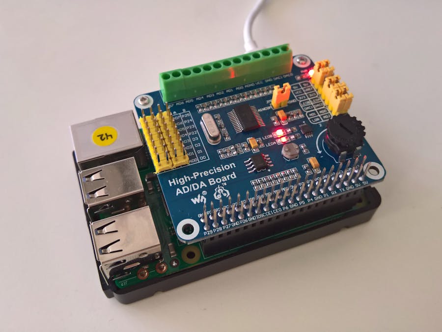
I got myself a Raspberry Pi High-Precision AD/DA Expansion Board to be used in a Windows IoT Core C# application.
The board has one 2-channel digital-to-analog converter chip (DAC8552) and a 8-channel analog-to-digital converter chip (ADS1256).
All documentation provided by WaveShare was referring to Raspberry Pi running Linux and the source code examples was written in C, so I had to write my own library. The first challenge was to try to understand how the Linux code actually communicated with the board, and it turned out to be quite a bit of detective work.
The Linux examples needed a BCM2835 library to work, so I started with its source code to get an understanding of it. It took some time to wrap my head around it, but in the end, it turned out not to be especially complicated.
Here are my findings.
The basics of the boardThe two converter chips both communicate with the Raspberry Pi over the SPI bus which uses three pins of the Pi: data in, data out and a clock signal.
Since the two chips share the same communication lines, somehow they need to know when the Pi wants to speak to the one or the other.
This is achieved by using two GPIO pins, one for each chip, controlled by the Raspberry Pi (who serves as the master of the communication). When the Pi is pulling the signal LOW on one of these pin means that the corresponding chip is selected. After communication, the signal is set back to HIGH. This is a common technique called chip select.
Now, simply put, by sending different commands over the SPI bus to the two chips, the Raspberry Pi is able to both set the voltage (between 0 and 5 V) on two different output terminals (using the DAC8552 chip) and read the voltage (between -5 and 5 V) on eight different input terminals (using the ADS1256 chip).
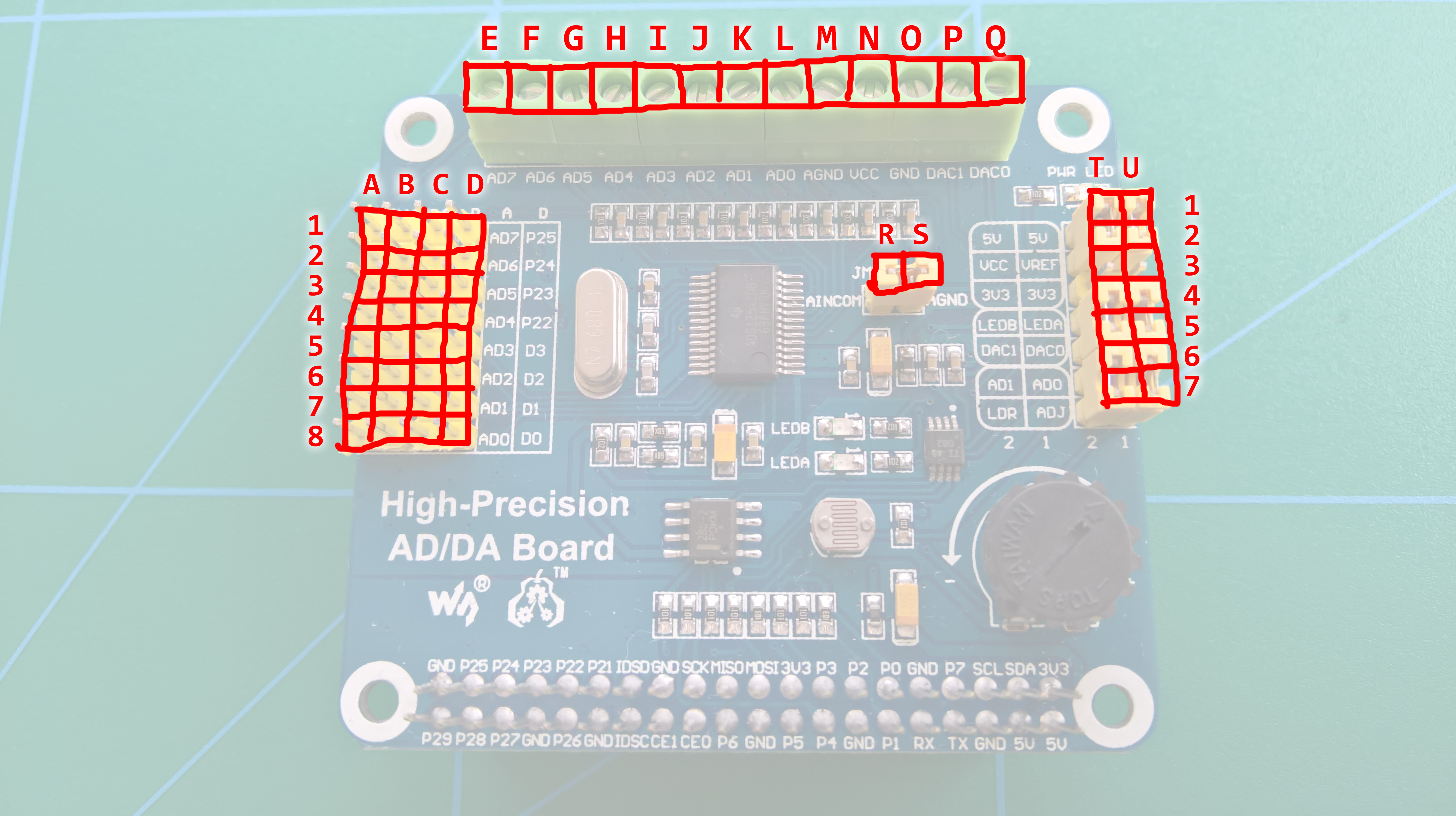
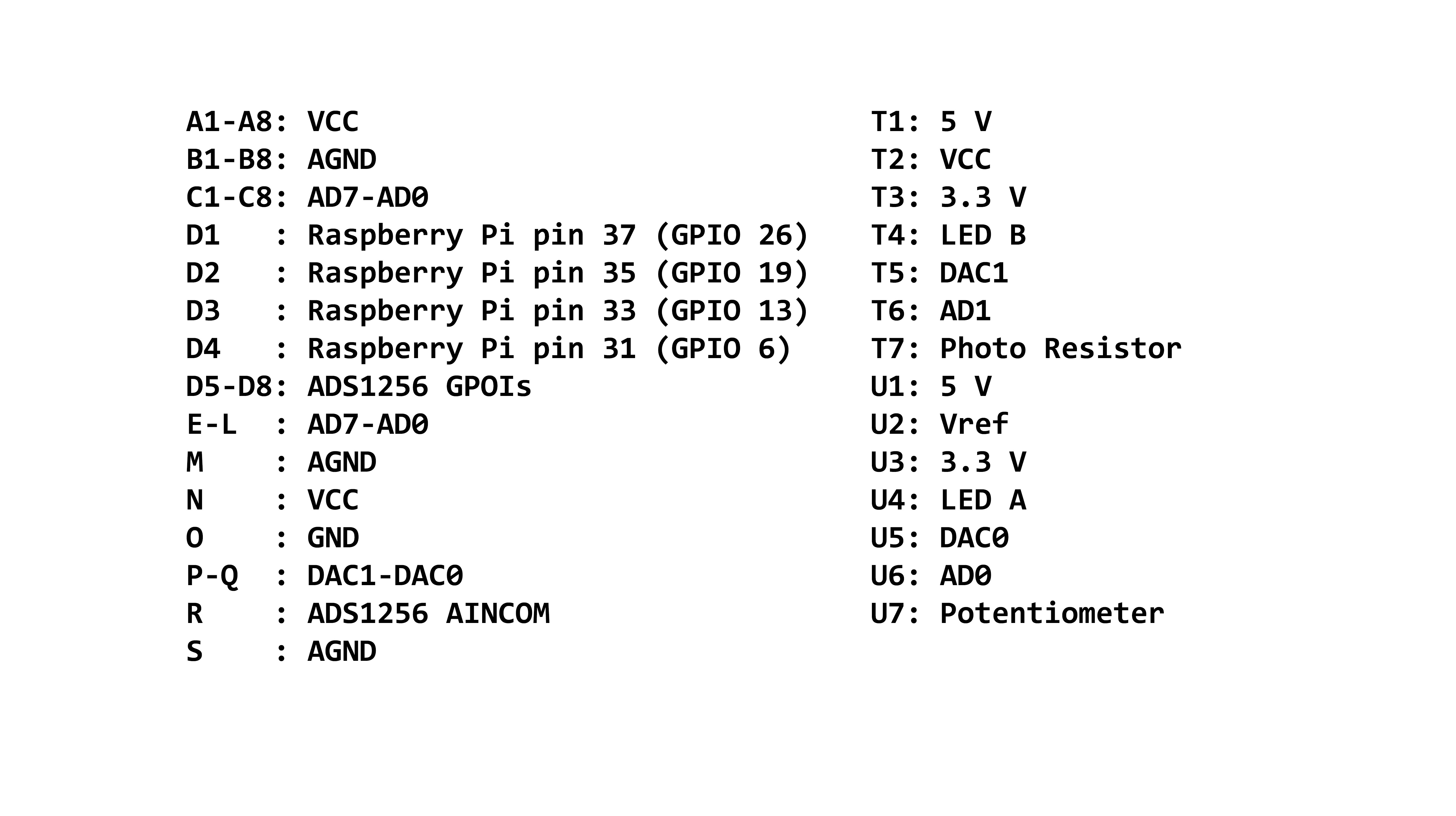
In the picture above, the input and output terminals are marked. The top green plastic bar consists of 13 screw terminals on which you can connect to both the analog input and output signals.
The yellow block of pins to the left is designed to fit Waveshare's different analog sensors.
The eight input pins are named AD0 to AD7 and the two output pins are named DAC0 and DAC1.
The basics of my code libraryEven though the two chips are on the same board I chose to put the code to handle them in different classes. This is mainly because they are dealing with totally different things.
They have, however, a common wrapper-class I named AdDaBoard (implementing the public IAdDaBoard interface). This class owns the two chip-specific classes Ads1256 and Dac8552, named after the two chips. These two classes implements the public interfaces IAnalogInput and IAnalogOutput, respectively.
To get an instance of the AdDaBoard you'll have to call GetAdDaBoard() on the static class AdDaBoardFactory instead of just creating a new instance. The reason is that the chip-communication requires the .NET class SpiDevice that must be instantiated asynchronously – and a .NET constructor (in this case for the AdDaBoard) cannot be asynchronous.
I wanted a clear and foolproof handling of the SPI bus. Codewise, I wanted to:
- Make sure only one of the two chips could use the SPI at any given time
- Automatically controlling the output level of the two chip select pins
In the end, I constructed a SpiComm class managed by a SpiCommController. There is one SpiComm instance for each chip.
The SpiComm implements the public ISpiComm interface which has two versions of an Operate method. The Operate methods takes a lambda expression that temporarily gives access to the actual .NET SpiDevice class. One of the methods returns a value (of any type) and the other one doesn't.
Calling Operate will first enter a lock statement, locking on a shared object for both the SpiComm classes. This ensures that the two SpiComm's cannot operate the SPI bus simultaneously. The second thing that happens is that the chip select pin is given a low output signal. Now the SpiDevice is handed over to the calling code, and when it returns the chip select pin is changed back to high and the lock is released.
Both the IAnalogInput and IAnalogOutput has the ISpiComm as a public property– this way the end user (you!) can gain access to the "raw" SPI bus exactly as the library code does. The reason is that my library is not fully complete; there are a number of features of the ADS1256 and DAC8552 chips that I left out.
The analog output converter was the easiest chip to get to work. To specify one of the output voltage levels all it took was to send three bytes to the chip.
The first byte is a set of control bits: determining which of the two outputs to affect, and if the voltage value should only be stored in the chip's internal buffer or actually going out on the pin.
The last two bytes holds the output voltage as a 16-bit number. A value of 0x0000 means the lowest possible output voltage (which is the same as GND; normally 0 Volt) and 0xFFFF means the highest possible (which is the same as Vref, normally 3.3 or 5 Volt).
The Vref voltage can be easily switched between 3.3 Volt and 5 Volt using a jumper on the board:
Placing the jumper covering the top two pins (of the three marked above) connects 5 Volt to the Vref connection, and placing it covering the bottom two pins connects 3.3 Volt.
(The middle pin of the three is the Vref, and I assume you can connect it to other reference voltages.)
In my library code, I chose to have two ways of specifying the output voltage; one taking the wanted voltage and the currently used Vref – and another taking the wanted normalized voltage (between 0.0 and 1.0). Both methods are called SetOutput but have different parameters.
There are also methods to be called to set both output values (SetOutputs). Doing this you ensure that the two outputs are changed at exactly the same time (if you would need that).
Take a look in the datasheet of the DAC8552 chip to see all the details. (Hint: they call the two output pins A and B.)
The analog input converterThe input converter chip ADS1256 was a bit more complicated. You can find the datasheet here. First of all, it required one more GPIO pin called Data Ready (or DRDY in the datasheet).
This is a signal the chip basically uses to tell the Pi if it's ready or not to accept new commands on the SPI bus. If the Pi reads a low level on the pin, it means the chip is ready. The behavior of the chip is controlled via a set of internal registers (see page 30 in the datasheet). In my library, I make use of the first four (although there are eleven in total).
The registers can be controlled via my library using the properties of the IAnalogInput. At startup, I read the registers and convert the current settings to the class properties.
Changing any of the properties does not have an immediate effect. It's not until a reading is done of any of the analog input pins that they are written to the registers (and they are only written if they have changed since the last reading).
Nothing will happen if any of the properties are changed during a reading (perhaps by another thread); the ongoing reading will use the property settings as they were when the reading began – the changed properties will affect the next reading.
One property is called AutoSelfCalibrate. This will make the chip re-calibrate before the next reading if any of the affected registers has changed since the last calibration. There is also a method called PerformSelfCalibration that will perform a calibration on demand. But I think the auto-calibration feature is the best.
The Gain property is an enum that can be used to magnify a smaller reading. Using a gain of 1 allows the input be in the full range of -5 V to +5 V. A gain of 2 allows only half of that range – but with twice the resolution. A gain of 4 allows an input in the range of ±1.25 V and the highest gain (64) can only read an input between ±78.125 mV (see page 16 in the datasheet; it's called PGA there, short for Programmable Gain Amplifier).
The DataRate is an interesting property. It specifies how fast the chip should sample the input levels. It also determines how much filtering should be applied, if I understand the datasheet correctly. A very fast data rate means less filtering and vice versa. More filtering means a more exact value. The highest rate is 30,000 samples per second, but in reality, you cannot squeeze these many readings out of the board – not on the Raspberry Pi running Windows 10 IoT Core, which is not a real-time operating system in this sense. This means, for instance, that the analog input is not very suitable for sampling sound. I guess you could, but you would get a very lo-fi result.
The effects of the data rate appears all over the datasheet. Search for "30,000" in the datasheet! There is a "open/short sensor detection" on the chip, and it is controlled via the DetectCurrentSources property. You can read more about this on page 15 in the datasheet.
The final property is the UseInputBuffer which controls whether to use the embedded input buffer or not. Read more about it on page 15 in the datasheet. It is a "low-drift chopper-stabilized", which sounds very cool, although I have no idea of what it means.
Reading an input value can be done in two ways: either by simply reading one of the eight pins (GetInput), or by getting a differential reading between two pins (GetInputDifference).
Either way, you need to specify the vRef parameter, but that is just to scale the returned value to the right level. It doesn't necessarily have to be the actual vRef voltage; it just sets the range of the returned value. For instance, if you say vRef is 1.0, you will get a reading between -1.0 and 1.0.
Thread safetyThe code should be completely thread-safe. You may call any method or change any properties from parallel threads without having to do your own locking.
Running the demosThe board comes with a couple of components that simplifies playing with both the inputs and outputs.
The blue marking shows two LEDs that can be connected to the output signals. To rewire the output signals to them, you must place a jumper marked with the green 1 and 2. (Jumper 1 is for the output pin DAC1 to LED B and jumper 2 is for output pin DAC0 to LED A.)
The big red marking is a potentiometer that may be connected to the input pin AD0 using the marked jumper 4. Turning the knob anticlockwise lowers the voltage on the first analog input pin, and turning it clockwise raises it.
The smaller red marking shows a photo resistor that may be connected to the input pin AD1 using the marked jumper 3. Exposing it to light will affect the voltage to the second input pin.
To run my demo application, RPi.AdDaBoard.Demo, all four jumpers should be connected (to make use of both the LEDs and both the input resistors).
In the constructor of the MainPage, you will find a simple way of choosing which demo to run. There is one simple output demo, one simple input demo and one that combines both input and output.
The output demo makes the LED lights alternately go from completely off to full brightness and back repeatedly. The input demo reads the voltage levels of the potentiometer knob and the photoresistor and writes the values to the Visual Studio debug output console. The input/output demo is a blend of the two; it takes a reading of the potentiometer knob and puts the value to the LEDs.
The demo code should be easy enough to understand how to use the library, but don't hesitate to ask questions!


Comments
Please log in or sign up to comment.