Light and Air Prove Dope Enough for Low-Cost, Environmentally-Friendly Semiconductor Devices
Designed to do away with expensive, environmentally-damaging, and hard-to-handle dopants, this photocatalytic approach shows promise.

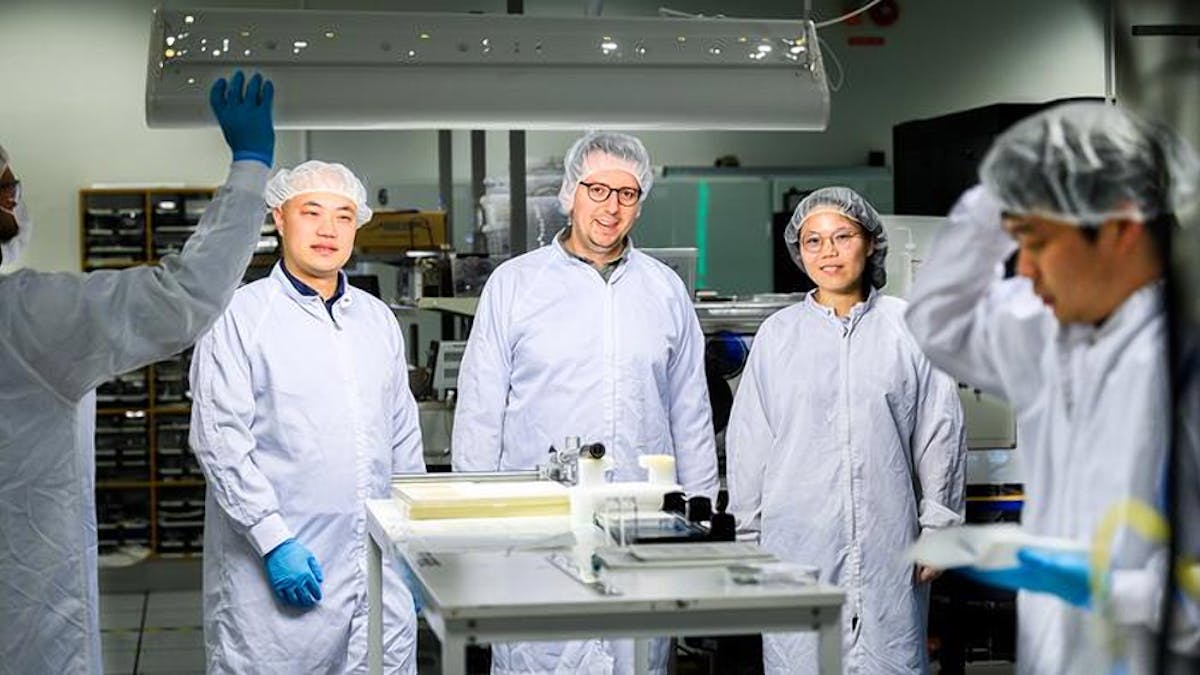
Researchers from Linköping University, the University of Groningen, the Università degli Studi di Cagliari, Korea University, Imperial College London, Università di Roma, and the Georgia Institute of Technology have come up with a novel approach to making electronics less damaging to the environment — by creating air-doped organic semiconductors.
"Our approach was inspired by nature, as it shares many analogies with photosynthesis, for example. In our method, light activates a photocatalyst, which then facilitates electron transfer from a typically inefficient dopant to the organic semiconductor material. We believe this method could significantly influence the way we dope organic semiconductors," claims Simone Fabiano, associate professor at Linköping University and co-corresponding author on the paper detailing the team's work.
"All components are affordable, easily accessible, and potentially environmentally friendly, which is a prerequisite for future sustainable electronics."
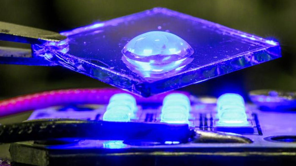
Traditional semiconductor devices are created by "doping" a silicon substrate using a range of chemical additives — materials that can be environmentally damaging, difficult to produce and handle, and expensive. The team's approach swaps the silicon for a plastic substrate and the traditional dopants for air and light.
The team's approach sees a conductive plastic substrate dipped into a salt solution that serves as a photocatalyst, with the doping process triggered by exposure to light and air. Oxygen from the air reacts with the plastic, creating a p-type semiconductor — and the salt solution can be reused again and again, making it both cost-effective and environmentally-friendly.
"It's also possible to combine p-doping and n-doping in the same reaction, which is quite unique," Fabiano adds. "This simplifies the production of electronic devices, particularly those where both p-doped and n-doped semiconductors are required, such as thermoelectric generators. All parts can be manufactured at once and doped simultaneously instead of one by one, making the process more scalable."
"We are at the beginning of trying to fully understand the mechanism behind it and what other potential application areas exist," Fabiano admits. "But it’s a very promising approach showing that photocatalytic doping is a new cornerstone in organic electronics."
The team's work has been published in the journal Nature under open-access terms.
Main article image courtesy of Thor Balkhed.
Freelance journalist, technical author, hacker, tinkerer, erstwhile sysadmin. For hire: freelance@halfacree.co.uk.