Use Your Resin 3D Printer to Fabricate PCBs
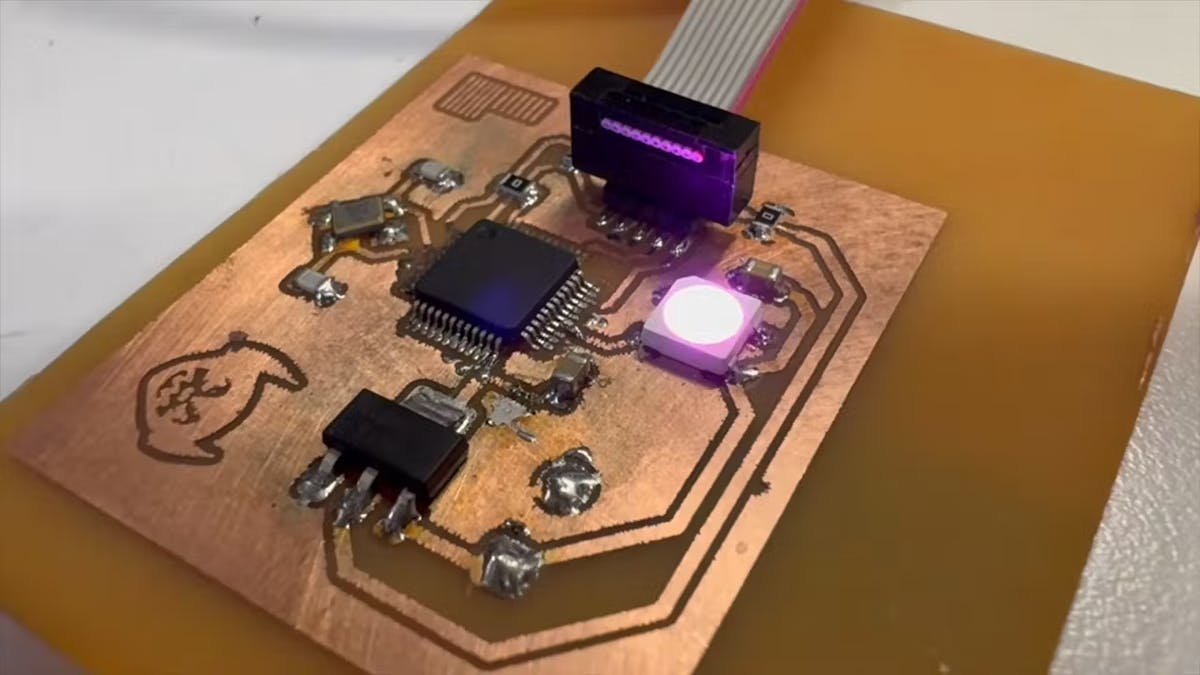
Stephen Hawes has a great video demonstrating a technique for making custom PCBs using a Formlabs SLA resin printer.

There has never been a better time for makers to get high-quality PCBs manufactured overseas at dirt cheap prices. But sometimes you don’t want to wait for fabrication and shipping. Sometimes you just want a simple PCB right now, so you can test your design and make sure it works. Maybe you’ll use that in your final build, or maybe you’ll use it for prototyping and then switch to a professional PCB. In either case, you can follow this video guide from Stephen Hawes to make your own PCBs using a resin 3D printer.

Back in the old days before cheap professional PCB fabrication, makers used to create their own PCBs from blanks using a chemical etching process. Those blanks are just copper on substrate and the chemical etching dissolves away the unnecessary copper, leaving just the useful traces and pads behind. The trick is dissolving just the unwanted copper and not the copper you want to keep.

There are several techniques for achieving that and they rely on “masking” the copper you don’t want the chemical etchant to touch. One classic method is printing (on a regular laser printer) and transferring the toner onto the copper as a mask.
This method shown by Hawes works in a similar way, except it “prints” the mask directly onto the copper using the UV light from a resin 3D printer. Hawes used a Formlabs printer for the job, but any modern SLA or MSLA printer model should work.
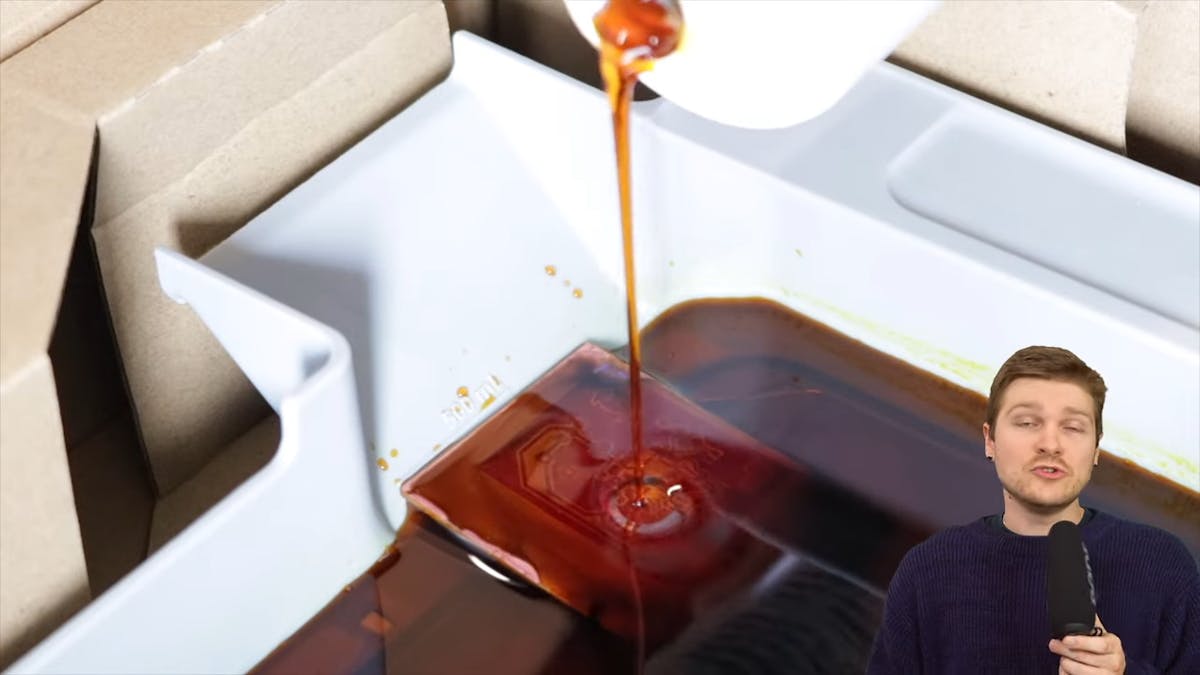
Instead of toner, this technique calls for UV-sensitive film. That covers the copper, then the UV light from the printer exposes the mask and leaves the traces and pads protected. A quick wash in water removes the uncured portion of the mask and then a ferric chloride bath etches away that unprotected copper. Finally, acetone removes the cured film.
The biggest challenge is getting the print settings right. As far as the printer knows, it is just curing a resin part. So, you have to tweak the settings to properly cure the UV film. Too little exposure and you don’t get a good mask. Too much exposure and you’ll oversize the mask, resulting in nearby pads and traces touching each other.
And, of course, unless you drill holes, then this will just be for SMD parts. But if you want a prototype PCB immediately, it is hard to beat the convenience of this technique.
Writer for Hackster News. Proud husband and dog dad. Maker and serial hobbyist. Check out my YouTube channel: Serial Hobbyism


