


Hardware components | ||||||
| × | 1 | ||||
| × | 1 | ||||
| × | 1 | ||||
Software apps and online services | ||||||
| ||||||
This is an FPGA beginners guide meant for absolute beginners who are just getting started. This is meant as a Tutorial to help you in making your first FPGA projects, by demonstrating the implementation of a simple example circuit 'Full Adder' using the VIvado Design Suite
However, this won't be the typical Verilog, or any HDL based tutorial. This guide uses 'Block Design' or IP-based designs for the tutorial. And this tutorial assumes the reader has no prior experience with a FPGA or with any HDLs. More on Why Block Design later. First, we'll see what a FPGA is, and why you should consider one for a project.
FPGA: What is it?An FPGA - Field Programmable Gate Array, is a part of the programmable logic devices family. To give you a bit of a backstory, in the very early days of digital electronics, if you wanted an IC for anything, that IC could do perform only a singular function throughout its entire lifespan, for example a 555 timer IC can only ever function as a timer or counter, not a adder.
These are fixed in purpose and cannot be used for anything else. It was only later on that programmable IC become mainstream but even then, most were One Time Programmable. Of the reprogrammable devices, such as PAL, PLC etc... FPGAs, due to their versatile nature and efficiency have made themselves an important role in many fields, particularly in prototyping.
In simpler terms, an FPGA can be seen as a more powerful version of common boards like Arduinos or Raspberry Pi, but only when you're not focusing on sequential program execution (step-by-step tasks).
FPGA vs MicroprocessorTo put it simply, a FPGA operates in 'parallel' while a Microcontroller, based on some Microprocessor, does so by repetitive cyclic execution of some basic instructions. Ex: Every operation would follow a cycle similar to the following in a Microprocessor :
Fetch;
Decode;
Execute;
However, FPGA is like physcial construct that does a specific function only so long as its programmed to do so. If it helps you imagine, then FPGA implements an OR gate like two rivers intersecting and forming a singular path for water flow. If there is water on either river, you get water from the final path. A microprocessor would test first river for water, then the second, then compare them, then place water on the final path. I hope you can see why FPGA is 'parallel' and thus faster, more reliable for real time application like in Defence, Industrial, Space crafts etc...
Once you have a different need, you can simply 'reprogram' the FPGA. Similar to a Embedded C library, you can use IP - Intellectual Properties in FPGAs to boost up your speed and performance of your project. All right, I thinks its time to get on with the Vivado tutorial.
Getting started with VivadoFirst, make sure you have all the requirements as mentioned above. You will need a copy of Vivado Design Suite installed on your PC and a ZedBoard at hand. If you don't have Vivado, you can install it for free from their official website here
Note you may need a AMD Account to download, install or both. You can get one for free from their Official Website.
When you open Vivado after installation, You will land in it's Overview page. You will see a Quick Start section under which Create Project option will be available. Click on it to create your new project. From there on, the porject creation process would be pretty straight forward. Just ensure you have selected the following:
- RTL Project (With Sources not specified option)
- ZedBoard is selected under Boards (Default parts window)
Now that you have created your porject, You will be landed in a windows similar to the following.
On the left side, you would see a IP Integrator section under the Flow Navigator. Under that option, click on Create Block Design. On the right side a new tab called Diagram would open.
Now you have created a Diagram - the canvas where you will draw your design using IP blocks.
On the Diagram tab's tool bar, you will see a + button. This button is for adding your IP (s) to your Design, and clicking on it will promt you to select IP by listing all available IP.
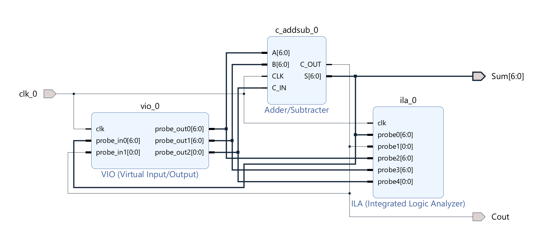
We plan to do a simple adder. A Adder will add given numbers and give out the sum as result. However, where and how can we access this result? There are two methods of viewing the result. Either by wiring the result to a set of LEDs, LCD displays etc.. or Internally using Vivado.
We will explore both options, and to do that you need an IP called ILA (Integrated Logic Analyzer) It is this ILA that allows you to view the specificed signal from the comfort of your vivado software.
And then you'd need the Adder/Subtracter IP and VIO (Virtual Input/Output) IP. VIO allows you to declare inputs and outputs, similar to what you would do in a HDL code based design. For example, it essentially replaces the following in a typical Verilog code.
input wire [7:0] a,b;
output reg [7:0] sum;
You Diagram should look like this at this part of the tutorial:
Now, you can double click on each block to open it's customization window, from which you can modify the IP to better suit your needs. For example, in the Adder Block, you can add a Carry In port, and a Carry out port, a Mode port for determining addition or subtraction operations. You can also define the width of data signals. I recommend to specify the A and B widths as 7, As we plan to view the result via the built-in LEDs of the ZedBoard. Also Disable CE (Clock Enable), while adding C_IN and C_OUT. And that should do it for the Adder Block.
Moving on, the process is similar for other blocks too.
Think of the VIO as a module, seperate from the Adder. You'd need to connect them together, in a way that output of one block would be the input of the other and vice versa. That is, Sum and C_OUT, while being outputs of the adder block, are infact seen as inputs when viewed from the VIO block. Therefore, you'd need to connect them in such a way to effectively hanlde the signals. And so, in the customization window, you will need to specify No. of Input probes as the total 'output' signals, and vice versa for No. of Output probes. Make sure you match the probe width too.
Now, wtih the ILA block, you'd Switch to Native in the Customization window, because we want to see signals that the FPGA sends outside its main logic fabrics. We'd use AXI if we wanted to see what was going on inside it's different fabrics.
Once thing to note here is declaring external signals. The clock to the circuit would be supplied by the global clock, generated by the FPGA, by default. Therefore, we can use that, and when we do, it will be a external signal supplied to the logic fabric. Hence the clock must be declared as external port/pin. You can do this by right clicking on any clk pin from one of the three IP blocks, then select 'Make External' in the menu that would pop up.
Now once you're done with this, all that's left is just connecting the signals. clk goes to all other clk. The output probe with width 7 goes to sum (S), the single bit one to C_OUT, and like so, for A, B and C_IN.
Up to this point, you have done enough to view your results via the ILA. You can stop here if that all you want, but seeing the results in the LEDs don't take much work from here.
You'd right click an empty space then choose Create Port. Then give a appropriate name such as 'Sum', and define that port as a output, of type data, and a vector of width 7 bits, that's 6:0. Then another one for Cout, following similar process.
On the left, you'd see a sources tab, wedged between the DIagram tab and the Flow Navigator. There, your '.bd' file should be visible. Right click on it to open the menu, and select Create HDL Wrapper. Once that's done, you are essentially 90% done with this example. In the sources tab, you will see a + option. Click on it will open the create files window. Select 'Constrainsts'. Once you have created a.xdc - Xilinx Design Constraint file, copy and paste the XDC code I have provided. These define which signals are mapped to which physical pin on the board, and at what voltage. And, make sure you either have same port name as me, or modify the XDC file to fit the port names you had given. Failing to match the ports will result in error, so make sure you have Matched them.
As you can imagine, this step is very important. In your future projects, make sure you get these pins right. To do so, you should refer to your FPGA manufacturer's page. Here is the link for ZedBoard's . You should find the ZedBoard Master XDC Rev C_D v3 under 'Programmable Logic Master User Constraints'
Once that's all done, you're good to click on that Generate Bitstream option. If you had did everything right, you'd get a window saying a bitstream file was successfully generated, and if you'd like to open Hardware Manager among other things. Choose HW and you should see a Open Target, select Auto Connect. Oh and Make sure you have connected the board to your computer, with correct cables and at correct ports (Connect the Micro USB to the JTAG port, right next to the Power Cable).
Once successfully detected, you will see a Program Device options. Select it, and go ahead and program your device. A Blue LED will light up, indication the Success Status of the program process.
Initially you will see the Waveform Window, titled as hw_ila. here you can see all the signals and their status, by clicking on the Trigger, which is run symbol, similar to a video pause button. Next to that tab, you will find hw_vios. And here is where the real deal happend. Select the + button and add all your signals. Once added you can freely manipulate their values, with their effects being immediately visible on the FPGA Board.
Congrats! You have done your First FPGA project.
You can refer to my PDF documentation, for a more Picture-by-Picture/step-by-step walkthrough on using Vivado here.


Comments
Please log in or sign up to comment.