


Hardware components | ||||||
_ztBMuBhMHo.jpg?auto=compress%2Cformat&w=48&h=48&fit=fill&bg=ffffff) |
| × | 1 | |||
 |
| × | 2 | |||
 |
| × | 16 | |||
 |
| × | 16 | |||
 |
| × | 1 | |||
 |
| × | 1 | |||
 |
| × | 1 | |||
Software apps and online services | ||||||
 |
| |||||
If you have arrived at this article by random means and not via its starting point, then you may find that it may not make much sense. This is because this article is one of several (six) tutorials to aid and assist in understanding the use of the ez_SIPO8_lib library in managing and controlling Serial-in/Parallel-out ICs (SIPOs) shift registers, for example 74HC595 chips.
If you wish to link to the start of the tutorial then please follow this link (Tutorial Start), otherwise, please read on...
A tutorial to consolidate understanding and use of the ez Serial-in/Parallel-out IC Library (ez_SIPO8_lib) - Tutorial 4, Cascading SIPOs. If you wish to link to the tutorial starting article then follow this link: Tutorial Start.You can access and download the User Guide, Crib Sheet and the original ez_SIPO8_lib article by following these links below:- ez_SIPO8_lib User Guide- ez_SIPO8_lib Crib Sheet- Read the full ez_SIPO8_lib articleIntroduction to the TutorialIn this tutorial we will look at configuring and driving two 8-bit SIPO ICs, i.e. two x 74HC595 IC, in a single cascade, to provide 16 outputs in a single SIPO bank.
ObjectivesIn this tutorial we shall build on what we have learned from previous tutorials and concern ourselves with creating a SIPO environment in which we can apply further basic principles to drive a single bank comprising two cascaded SIPO ICs. In particular we shall learn:
1. how we can wire up and cascade two 74HC595 ICs (SIPO ICs), as a single SIPO bank, to the microcontroller
2. how we are able to use some of the SIPO8 library functions/methods to drive the cascaded SIPO bank
3. how we can extend the two SIPO cascade model to any number of connected SIPOs in a single SIPO bank cascade
4. witness the outputs of the sketch – shifting LED patterns and serial monitor SIPO data.
If you ran through previous tutorials (Tutorials 1 or 2 or 3) and still have your components set up then extend your set up to add a further SIPO IC (74HC595) as below.
Kit ListGather together the following components:
- 1 x Arduino UNO - The design uses an Arduino UNO, but any suitable microcontroller (Arduino or clone) will do, providing it is able to support the pin out requirements for driving the SIPO interface and power requirements
- 1 or 2 x Breadboard - One or two breadboards to fit 2 x ICs, resistors and LEDs
- 2 x 74HC595 IC - 8-bit SIPO IC, or other clone providing it is genuinely ‘plug-compatible’
- 16 x LEDs - Whatever you have around
- 16x Resistors, 220 ohm - One per LED. Use 220 ohm resisters and ignore the suggested 180 ohm values in the wiring diagrams
- Connecting wires - Short/long or breadboard wire connectors, whatever suits. Short bridging wires are very useful in this wire up as it keeps cable clutter down.
Which end is which? Well, notice that the 74HC595 has a notch at one end, here at the top of the diagram. Pin numbering starts at 1 at the top left and continues down and the around the bottom of the IC rising to the top right hand side:
For this tutorial we shall be using an addition IC pin, QH’(serial out) on the first IC, to link to the second SIPO in our two SIPO cascade.
UNO/SIPO Interface Pin ConfigurationEvery bank of SIPO ICs you connect to the microcontroller requires a 3-wire digital interface. The table below suggests pin mappings between the microcontroller and the SIPO IC for this tutorial, but you may choose what microcontroller digital pins you wish. If you do choose different pins then be sure to alter the sketch create_bank call.
- UNO pin 8 to SIPO pin 14 - SIPO Data Pin
- UNO pin 9 to SIPO pin 12 - SIPO Latch Pin
- UNO pin 10 to SIPO pin 11 - SIPO Clock Pin
- UNO pin +5v to SIPO pins 10, 16 - Power to the SIPO
- UNO GND pin to SIPO pins 8, 13 - Return ground (0v)
Note that we use the same microcontroller digital pins for the SIPO IC cascade interface – no change required.
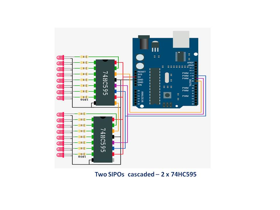
Connecting It All TogetherUsing the following diagram, wire up all of the components, taking care to get the output/input connections correct:
Take time to layout your components and try and keep to a logical order. It is very easy to get out of step and make incorrect connections. The illustration above provides all of the information required to complete the wiring up process. I recommend the following approach:
1. on the breadboard, position your two SIPO ICs in a convenient position and straddling the central break line. Orientate each SIPO correctly, note the notch indicating which end is which and where pin 1 starts
2. next position your LEDs and resistors on the same or another breadboard, convenient for wiring up to the SIPO output pins (remember, the SIPO ICs have all but one of their outputs on one side (SIPO pins 1–7)
3. now make all of the ground connections, followed by the power connections, see figure, above.
4. then connect all other pins together including the LEDs as per figure, above, except the 3-wire connections to the microcontroller
5. now carefully inspect your work and when happy...
6. connect the 3-wire interface wires as per UNO/SIPO Interface Pin Configuration table above. Top tip –colour code the 3-wire connectors, e.g. SIPO pin 14 – data/red, SIPO pin 12 –latch/white, SIPO pin 11 – clock/green, or any other colouring of your choice. This makes it easy to recall which wire is which when you connect to the microcontroller.
As a further tip, try and use breadboard connecting jumper/bridge cables where you can, it keeps things looking tidier and easier to work out where errors are.
The Code/SketchNow that is done, let’s look at a simple sketch to play around with the 75HC595 SIPO ICs.
Using the Arduino IDE, start with a new sketch and enter the following (download from the Code section):
//
//   Tutorial 4 - use of ez_SPI8 library,
//   2 x physical SIPOs, cascaded into a single SIPO bank
//
//   Ron D Bentley, Stafford, UK
//   April 2021
//
//   This example and code is in the public domain and
//   may be used without restriction and without warranty.
//
#include <ez_SIPO8_lib.h>
int bank_id;
#define Num_SIPOs   2
#define Num_timers  0
SIPO8 my_SIPOs(Num_SIPOs, Num_timers); // initiate the class for the tutorial
void setup() {
 Serial.begin(9600);
 // create a single bank of required number of SIPOs in the bank,
 // params are: data pin, clock pin, latch pin, number of SIPOs this bank
 bank_id = my_SIPOs.create_bank(8, 10, 9, 2);
 if (bank_id == create_bank_failure) {
   my_SIPOs.print_SIPO_data();
   Serial.println(F("failed to create bank"));
   Serial.flush();
   exit(0);
 }
 // print the bank data for confirmation/inspection
 my_SIPOs.print_SIPO_data();
}
// patterns to be xferred / shifted out to the SIPO bank
#define num_patterns 7
uint8_t patterns[num_patterns] = {// starting patterns
 0b11111111,
 0b00001111,
 0b00110011,
 0b01010101,
 0b11000011,
 0b01000010,
 0b00111100
};
void loop() {
 // scroll through every SIPO bank and assert the given pattern to every
 // SIPO defined by the bank.
 do {
   // setup each pattern in turn
   for (uint8_t pattern = 0; pattern < num_patterns; pattern++) {
     // perform 2 passes for each pattern - first, as defined, second inverted
     for (uint8_t cycle = 0; cycle < 2; cycle++) {
       // consider each SIPO in this 2 SIPO cascaded bank
       for (uint8_t sipo = 0; sipo < my_SIPOs.SIPO_banks[bank_id].bank_num_SIPOs; sipo++) {
         my_SIPOs.set_bank_SIPO(bank_id, sipo, patterns[pattern]); // set all pins of this SIPO in this bank_id
       }
       my_SIPOs.xfer_bank(bank_id, MSBFIRST);  // update physical SIPOs for this bank_id
       delay(500);
       patterns[pattern] = ~patterns[pattern];// invert current pattern byte for next pass
     }
   }
 } while (true);
}
Compile the sketch and upload. You should now see the LEDs performing the preset binary patterns.
Points to note:
1. there are few SIPO8 library functions/methods utilised in the sketch - create_bank, set_bank_SIPO, and xfer_bank. The sketch does include a print_SIPO_data function call so you are able to verify your setup data (see below example)
2. we make use of a native SIPO control structure variable value -
my_SIPOs.SIPO_banks[bank_id].bank_num_SIPOs,
although we could have simply stated “2” as the number of SIPOs within the SIPO bank. This is demonstrated here as a help for future projects where you may be dealing with many SIPO banks concurrently each bank with many SIPO ICs – it makes the method self maintaining.
3. note the use of the invert operator (~) which is used to invert the current bit pattern data each pass.
Finally, check the serial monitor, it should look like this:
SIPO global values:
pins_per_SIPO = 8
max_SIPOs = 2
bank_SIPO_count = 2
num_active_pins = 16
num_pin_status_bytes = 2
next_free bank = all SIPOs used
Number timers = 0
Bank data:
  bank = 0
    num SIPOs = 2
    latch_pin = 9 clock_pin = 10 data_pin = 8
    low_pin = 0 high_pin = 15
Note the helpful details that print_SIPO_data() function can provide – very useful during development and debugging.
Have a play around varying the patterns, reducing the sketch to a single SIPO bank, adding more SIPO ICs to your two SIPO bank cascade, adding more banks, etc. The most difficult aspect of using SIPO ICs is the number of cables/connections needed –a tidy mind helps.
That is the end of Tutorial 4 which I hope you have found to be instructional. A copy of the tutorial can be downloaded from github here.
If you are ready and wish to go on to the next tutorial then follow this link: Tutorial 5, Bank Interleaving, but if you wish to link to the tutorial starting article then follow this link: Tutorial Start.

Comments
Please log in or sign up to comment.