


Hardware components | ||||||
_ztBMuBhMHo.jpg?auto=compress%2Cformat&w=48&h=48&fit=fill&bg=ffffff) |
| × | 1 | |||
 |
| × | 1 | |||
 |
| × | 8 | |||
 |
| × | 8 | |||
 |
| × | 1 | |||
 |
| × | 1 | |||
Software apps and online services | ||||||
 |
| |||||
If you have arrived at this article by random means and not via its starting point, then you may find that it may not make much sense. This is because this article is one of several (six) tutorials to aid and assist in understanding the use of the ez_SIPO8_lib library in managing and controlling Serial-in/Parallel-out ICs (SIPOs) shift registers, for example 74HC595 chips.
If you wish to link to the start of the tutorial then please follow this link (Tutorial Start), otherwise, please read on...
A tutorial to consolidate understanding and use of the ez Serial-in/Parallel-out IC Library (ez_SIPO8_lib) - Tutorial 5, Bank Interleaving. If you wish to link to the tutorial starting article then follow this link: Tutorial Start.
You can access and download the User Guide, Crib Sheet and the original ez_SIPO8_lib article by following these links below:- ez_SIPO8_lib User Guide- ez_SIPO8_lib Crib Sheet- Read the full ez_SIPO8_lib articleIntroduction to the TutorialIn this tutorial we will look at bank interleaving. Bank interleaving allows us to define a number of identically sized SIPO banks but all sharing the same 3-wire microcontroller interface. This provides us with the means to maintain SIPO banks with different SIPO output pin configurations and xfer them to the same physical SIPO ICs, singly or as a multiple cascade, as our project dictates.
In this tutorial we shall concern ourselves with creating a virtual software SIPO environment in which we can explore/learn:
1. if the basic test harness is not already to hand from previous tutorials, how we can wire up and connect a single 74HC595 IC (SIPO) to a microcontroller, to test out some of the features covered by the tutorial
2. how we can create multiple SIPO banks, each with a different output pin status configuration/profile
3. how we can use the technique of bank interleaving to good effect, in this tutorial we shall revisit the User Guide sketch example of strobing LEDs
4. witness the outputs of the sketch configuration – strobing and sketch data structures/values
If you ran through Tutorials 1 and 2 and still have your components set up as for that tutorial, then skip to The Code/Sketch, otherwise continue as below.
Kit ListGather together the following components:
- 1 x Arduino UNO - The design uses an Arduino UNO, but any suitable microcontroller (Arduino or clone) will do, providing it is able to support the pin out requirements for driving the SIPO interface and power requirements
- 1 x Breadboard - Small or large, whatever you have to hand
- 1 x 74HC595 IC - 8-bit SIPO IC, or other clone providing it is genuinely ‘plug-compatible’
- 8 x LEDs - Whatever you have around
- 8 x Resistors, 220 ohm - One per LED. Use 220 ohm resisters and ignore the suggested 180 ohm values in the wiring diagrams
- Connecting wires - Short/long or breadboard wire connectors, whatever suits
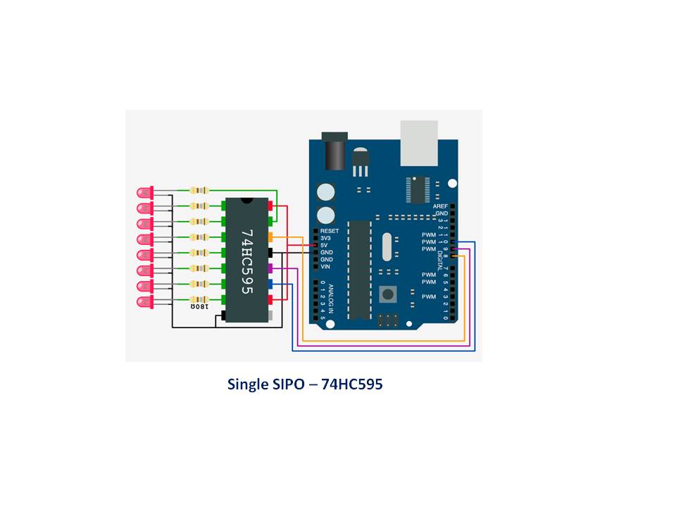
Which end is which? Well, notice that the 74HC595 has a notch at one end, here at the top of the diagram. Pin numbering starts at 1 at the top left and continues down the left hand side and the around the bottom of the IC rising to the top right hand side to pin 16:
Every bank of SIPO ICs you connect to the microcontroller requires a 3-wire digital interface (3WI). As this tutorial concerns a single SIPO IC then we shall only need one x 3WI. The table below suggests pin mapping between the microcontroller and the SIPO IC for this tutorial, but you may choose what microcontroller digital pins you wish. If you do choose different pins then be sure to alter the sketch function create_bank call in setup().
- UNO pin 8 to SIPO pin 14 - SIPO Data Pin
- UNO pin 9 to SIPO pin 12 - SIPO Latch Pin
- UNO pin 10 to SIPO pin 11 - SIPO Clock Pin
- UNO pin +5v to SIPO pins 10, 16 - Power to the SIPO
- UNO GND pin to SIPO pins 8, 13 - Return ground (0v)
Using the following diagram, wire up all of the components, taking care to get the output/input connections correct:
Notice that the only 74HC595 IC pin not to have anything connected is pin 9, QH’. This is used as the serial output pin to connect to the serial input pin, 14SER, of the next SIPO 74HC595 in a cascade.
The Code/SketchOkay, now let’s look at a sketch to strobe the LEDs connected to a single SIPO IC back and forth. In this version we shall use bank interleaving such that:
1. we will create eight single virtual SIPO banks. Note that these banks will be themselves virtual as they will all map to the same physical SIPO IC as they will use the same 3WI.
2. each (virtual) bank will be configured with a single pin, set HIGH. For example, bank id 0 will have pin 0 set High, all other pins in the bank being set LOW (relative addressing), bank id 1 will have pin 1 set High, all other pins set LOW, etc., thus bank SIPO pin settings will be (a strobing/sliding pattern across the eight banks):
- bank id 0 SIPO byte pattern
0b00000001
- bank id 1 SIPO byte pattern
0b00000010
- bank id 2 SIPO byte pattern
0b00000100
- bank id 3 SIPO byte pattern
0b00001000
- bank id 4 SIPO byte pattern
0b00010000
- bank id 5 SIPO byte pattern
0b00100000
- bank id 6 SIPO byte pattern
0b01000000
- bank id 7 SIPO byte pattern
0b10000000
3. we will simply xfer each bank in sequence to produce our strobing effect, starting at bank id 0 and at the end of each complete cycle of eight xfers, switch the direction of the shift out, thereby achieving a forward and reverse strobe.
4. witness the outputs of the sketch – strobing LED patterns and serial monitor SIPO data.
Download the sketch from the Code section:
//
//   Tutorial 5 - use of ez_SPI8 library,
//   Demonstration of SIPO bank interleaving - 8 x  SIPOs
//   each mapped to an individual bank but with the same 3-wire digital
//   pin microcontroller interface.
//
//   The sketch sets up each single SIPO bank with a different binary 8bit
//   (8 pin) pattern which is then xferred to the physical single SIPO IC.
//   The sketch mimics the strobe sketch by using bank interleaving.
//   To note is the small amount of SIPO8 library code that is used.
//
//   Ron D Bentley, Stafford, UK
//   April 2021
//
//   This example and code is in the public domain and
//   may be used without restriction and without warranty.
//
#include <ez_SIPO8_lib.h>
int bank_id;
#define Num_SIPOs   8
#define Num_timers  0
SIPO8 my_SIPOs(Num_SIPOs, Num_timers); // initiate the class for the tutorial
uint8_t bank_ids[Num_SIPOs]; // one bank_id per SIPO bank
uint8_t bank;
void setup() {
 Serial.begin(9600);
 // create banks of 1 x SIPO, all of same 3-wire interface and initialise
 // with each strobe pattern - 0b00000001, 0b00000010, 0b00000100, etc.
 // create_bank params are: data pin, clock pin, latch pin, number of SIPOs this bank
 for (bank = 0; bank < Num_SIPOs; bank++) {
   bank_ids[bank] = my_SIPOs.create_bank(8, 10, 9, 1);
   if (bank_ids[bank] == create_bank_failure) {
     Serial.println(F("failed to create bank"));
     Serial.flush();
     exit(0);
   }
   // now set up the strobe patterns in the bank's single SIPO, relative SIPO address is 0
   // sliding pattern of 1's starting at 0b00000001
   my_SIPOs.set_bank_SIPO(bank_ids[bank], 0, 1 << bank); // set up this bank's strobe pattern
 }
 // print the bank data and pin statuses for confirmation/inspection
 my_SIPOs.print_SIPO_data();
 my_SIPOs.print_pin_statuses();
}
void loop() {
 // scroll through every SIPO bank (interleave) and xfer the bank's pins
 // according to the direction for shift out.
 bool msb_or_lsb = MSBFIRST; // starting direction
 do {
   for (bank = 0; bank < Num_SIPOs; bank++) {
     my_SIPOs.xfer_bank(bank, msb_or_lsb); // xfer out this bank's SIPO pins
     delay(50);
   }
   msb_or_lsb = !msb_or_lsb; // switch direction
 } while (true);
}
Notice how succinct the sketch is. We do not have to do too much work to get the effect we set out to achieve. It demonstrates quite nicely the use of the shift out directional parameter MSBFIRST and !MSBFIRST (LSBFIRST). The key is in declaring virtual banks, each connecting to the same 3WI, i.e. a single physical SIPO IC.
Check the serial monitor, it should look like this:
SIPO global values:
pins_per_SIPO = 8
max_SIPOs = 8
bank_SIPO_count = 8
num_active_pins = 64
num_pin_status_bytes = 8
next_free bank = all SIPOs used
Number timers = 0
Bank data:
bank = 0
 num SIPOs = 1
 latch_pin = 9 clock_pin = 10 data_pin = 8
 low_pin = 0 high_pin = 7
bank = 1
 num SIPOs = 1
 latch_pin = 9 clock_pin = 10 data_pin = 8
 low_pin = 8 high_pin = 15
bank = 2
 num SIPOs = 1
 latch_pin = 9 clock_pin = 10 data_pin = 8
 low_pin = 16 high_pin = 23
bank = 3
 num SIPOs = 1
 latch_pin = 9 clock_pin = 10 data_pin = 8
 low_pin = 24 high_pin = 31
bank = 4
 num SIPOs = 1
 latch_pin = 9 clock_pin = 10 data_pin = 8
 low_pin = 32 high_pin = 39
bank = 5
 num SIPOs = 1
 latch_pin = 9 clock_pin = 10 data_pin = 8
 low_pin = 40 high_pin = 47
bank = 6
 num SIPOs = 1
 latch_pin = 9 clock_pin = 10 data_pin = 8
 low_pin = 48 high_pin = 55
bank = 7
 num SIPOs = 1
 latch_pin = 9 clock_pin = 10 data_pin = 8
 low_pin = 56 high_pin = 63
Pin status byte data –
Active pin array, pin statuses:
Bank 0: MS00000001LS
Bank 1: MS00000010LS
Bank 2: MS00000100LS
Bank 3: MS00001000LS
Bank 4: MS00010000LS
Bank 5: MS00100000LS
Bank 6: MS01000000LS
Bank 7: MS10000000LS
Before finishing this tutorial:
Have a go at varying the SIPO bit/pin patterns to get different effects.
Q. what would be the result if themy_SIPOs.xfer_bank(bank,msb_or_lsb)call in the main loop was replaced withmy_SIPOs.xfer_banks(bank,bank, msb_or_lsb)ormy_SIPOs.xfer_array(msb_or_lsb)?
A.my_SIPOs.xfer_banks(bank, bank, msb_or_lsb)will work just fine because the same single bank is being shifted out. However,my_SIPOs.xfer_array(msb_or_lsb)will not work because this function xfers all defined virtual banks (all eight!) in one go – not what we want.
That is the end of Tutorial 5, which I hope you found instructional. A copy of the tutorial can be downloaded from github here.
If you are ready and wish to go on to the next tutorial then follow this link: Tutorial 6, Questions & Answers, but if you wish to link to the tutorial starting article then follow this link: Tutorial Start.

Comments
Please log in or sign up to comment.