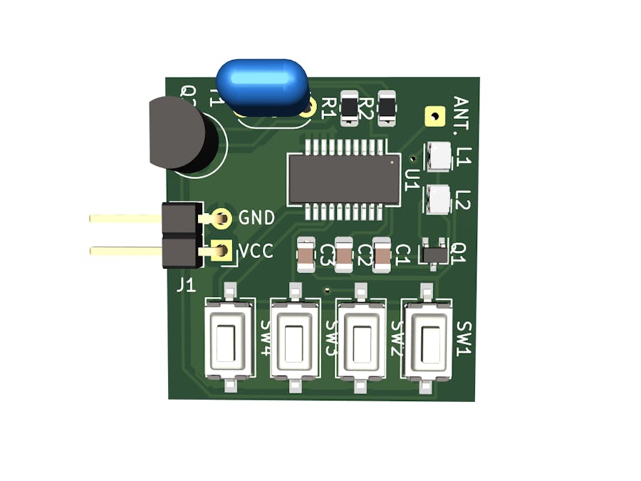
Two devices can communicate with each other using radio frequencies and using an RF transmitter is one of the simplest ways to do it. Various compatible ranges within the RF communication system range from 30 kHz to 300 GHz. The communication system’s digital data is constituted as disparities within the carrier wave’s amplitude; thus, the representation and modulation are referred to as the Amplitude Shifting Key (ASK).
Conceptualization of the ProjectTo conceptualize the 433 MHz RF Transmitter, a four-push button switch in an RF wireless medium will be used to control the 4 LEDs. The four push buttons are attached to an IC encoder. The primary function of the IC encoder is to get 4-bit data from each of the four push buttons and later transform it into serial data. The IC encoder also transmits the acquired 4-bit data with the help of an RF transmitter.
A Block Diagram of RF TransmitterComponents
A 433 MHz RF Transmitter, an HT12D encoder IC, four push buttons, LEDs, Jumper wires, an Arduino board, a 7805 Voltage Regulator, ohm Resistors, a Ceramic Capacitor, and a 9V battery that has a battery cap.
The tools used to attach the components include a soldering Iron, wire, flux, stand, wire cutter, multi-meter, and a de-soldering pump.
433 MHz RF Transmitter Circuit Diagram.
- AE1 1 Antenna Antenna Connector_Wire:SolderWire-0.1sqmm_1x01_D0.4mm_OD1mm Antenna
- C1 1 22uF C_Small Capacitor_SMD:C_0805_2012Metric Unpolarized capacitor, small symbol
- C2, C3 2 C_Small C_Small Capacitor_SMD:C_0805_2012Metric Unpolarized capacitor, small symbol
- J1 1 Screw_Terminal_01x02 Screw_Terminal_01x02 Connector_PinHeader_2.54mm:PinHeader_1x02_P2.54mm_Horizontal Generic screw terminal, single row, 01x02, script generated (kicad-library-utils/schlub/autogen/connector/)
- L1 1 7.5T, d=4mm L_Small Inductor_SMD_Wurth: L_Wurth_WE-LQSH-2010 Inductor, small symbol
- L2 1 2.5T, d=4mm L_Small Inductor_SMD_Wurth: L_Wurth_WE-LQSH-2010 Inductor, small symbol
- Q1 1 2SC3357 2SC4213 Package_TO_SOT_SMD: SOT-323_SC-70 0.3A Ic, 20V Vce, NPN Transistor, For Muting and Switching, SOT-323
- Q2 1 BC546 BC546 Package_TO_SOT_THT: TO-92_Inline 0.1A Ic, 65V Vce, Small Signal NPN Transistor, TO-92
- R1, R2 2 47k R_Small_US Resistor_SMD: R_0805_2012Metric Resistor, small US symbol
- SW1, SW2, SW3, SW4 4 SW_SPST SW_SPST Button_Switch_SMD: SW_Tactile_SPST_NO_Straight_CK_PTS636Sx25SMTRLFS Single Pole Single Throw (SPST) switch
- U1 1 HT12E HT12E Package_SO: SSOP-20_3.9x8.7mm_P0.635mm 2^12 serial encoder, SOP-20
- Y1 1 433MHz Crystal_GND2_Small Crystal: Resonator-3Pin_W6.0mm_H3.0mm Three-pin crystal, GND on pin 2, small symbol
Circuit Illustration
The VSS terminal of the HT12E encoder IC is connected to GND, whereas the VDD terminal is connected to VCC. Connecting pins IC A0–A7 (pins 1–8) to the ground (-) sets the address to 0b00000000. For example, pin 13 of AD11 is linked to Switch 1, pin 12 of AD10 is connected to Switch 2, pin 11 of AD9 is linked to Switch 4, and pin 10 of AD8 is linked to Switch 1. To facilitate the operation of the HT12E IC's internal oscillator, an external 1M ohm resistor is wired between pins 15 and 16. The negative (GND) terminal of the RF Transmitter module is connected to the negative (GND) terminal of the power supply. In contrast, the positive (VCC) terminal is linked to the power supply’s positive (VCC) terminal. The DOUT (pin 17) of the IC is wired to the Data pin.
How the 433 MHz RF Transmitter OperatesThe HT12E encoder IC interfaces with four push buttons through its 4 data pins. These push buttons are sources of 4-bit data input to the HT12E encoder IC. Subsequently, the IC processes this 4-bit data into serial data, which can be accessed at the IC's DOUT pin (pin 17). The resulting serial data is then directed to the RF Transmitter module, which utilizes radio signals to transmit this serialized information. The 433 MHz RF transmitter works with the RF receiver after power is supplied on the two circuits. After the power is provided, the LED starts to glow due to the Encoder IC pulling up the four push-button pins, i.e., the IC pin D8 to D11 internally. Pressing a single push-button in the transmitter circuit connects the data pin to the ground. Consequently, the corresponding LED in the receiver circuit will be switched off.
These excellent projects can be manufactured through PCBWay, a world-class fabrication house that has you covered anytime, anywhere in the world. PCBWay is holding the PCBWay 6th Project Design Contest, where electrical and mechanical engineering participants are allowed to participate. To participate, you must submit your project through their portal. Before submitting the project, ensure you understand this page's overview, pricing and rules, submissions, and discussions.


_4YUDWziWQ8.png?auto=compress%2Cformat&w=48&h=48&fit=fill&bg=ffffff)

_Ujn5WoVOOu.png?auto=compress%2Cformat&w=40&h=40&fit=fillmax&bg=fff&dpr=2)


Comments
Please log in or sign up to comment.