


_4YUDWziWQ8.png?auto=compress%2Cformat&w=48&h=48&fit=fill&bg=ffffff)
This project documents the development board's schematic and hardware layout.
An ATmega128RFA1 board has the following features;
Arduino-compatible with R3 Form Factor
Onboard chip antenna
33 Digital I/Os
SPI, TWI, and UART interfaces
8 Analog Inputs (10-bit)
16 MHz operating frequency
Pre-programmed ATmegaBOOT bootloader
On-board 3.3V regulator
ATmega128RFA1 with 6 Timers, 128 KB Flash, 16 KB SRAM, 4096 Bytes EEPROM
2.4 GHz RF Transceiver
RequirementsTo develop an ATmega128RFA1 board, gather SparkFun FTDI breakout, headers, power connector, and soldering tools for assembly.
What is an ATmega128RFA1?
Two parts are combined to make an ATmega128RFA1 board; both the half RF transceiver and the half microcontroller.
Half Microcontroller
In other words, it is known as the ATmega128, which is an enduring tradition of Atmel AVR microcontrollers. This microcontroller has a 128kB flash, numerous I/O pins, ADC, and more.
Half RF Transceiver
The unique ATmega128RFA1 transceiver, operating on a 2.4GHz wireless radio chip, enables communication within a 75m radius at 2 Mb/s. Supporting IEEE 802.15.4, it forms a PAN like Bluetooth but with a lower data rate (around 250kbps). Ideal for low-level, low-power, and low-range device communication, it suits various embedded applications like weather stations or remote coffee machine activation.
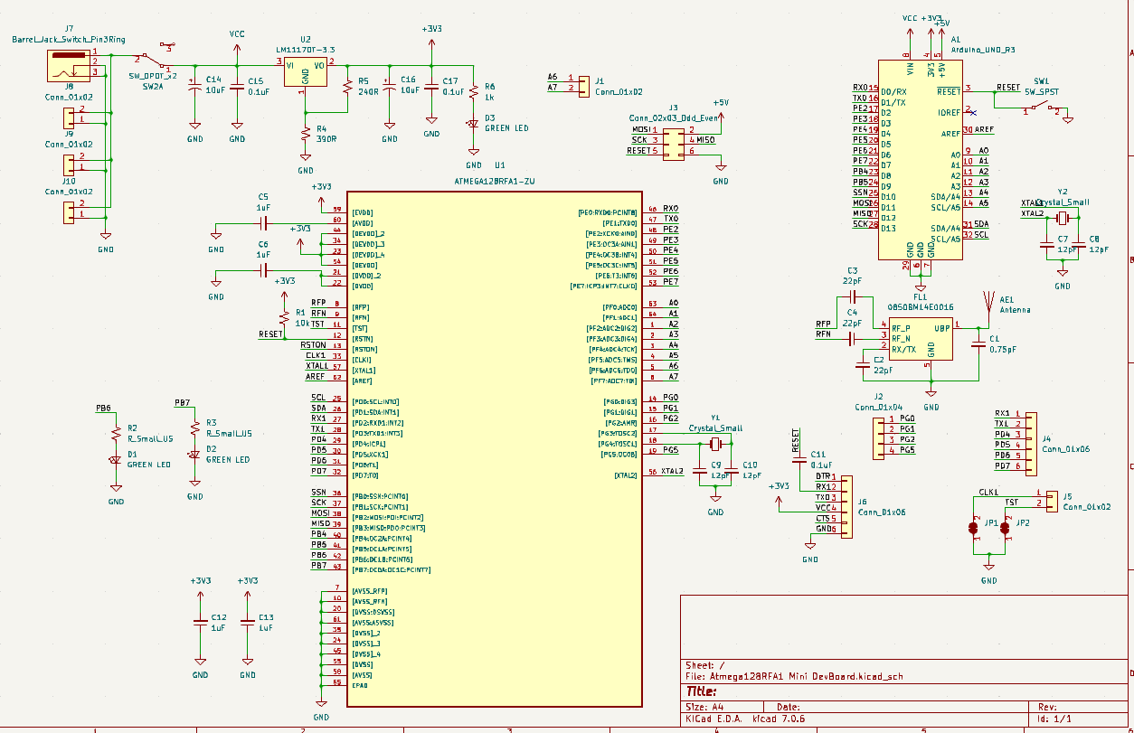
Schematic DiagramInput power
The circuit receives regulated 3.3V power from a voltage regulator. It has various input options like DC Barrel Jack, JST connector, screw terminal, and standard header, with a slide switch for power control. Also, it offers 3.3V and GND pins for voltage use.
Connectivity
The ATmega128RFA1 is supported by a 16MHz crystal and decoupling caps. The board has an RF section with a crystal, chip antenna, and supporting circuitry. Ensure antenna signal strength by avoiding component interference. Digital I/O pins, LEDs, and convenient analog inputs are available, resembling Arduino. The board features two programming headers: a 6-pin ICSP header for AVR programming and a 6-pin serial header compatible with standard FTDI headers and cables.
Board Powering
The board can be powered via various input jacks (barrel, JST, screw, 0.1" connectors). Voltage should be 4.5-15V, regulated to 3.3V. A 5V or 9V wall wart works with the barrel jack. The chip operates between 1.8 and 3.6V, with low power consumption for RF data (16-18mA) and idling (1-4.5mA). Output pins handle 2-8mA.
Serial bootloader
Bootloaders facilitate easy code uploading to chips, replacing costly programmers. The ATmega128RFA1 Development Board has a pre-programmed serial bootloader, allowing code upload via serial port or USB-to-Serial converter (FTDI Basic board recommended). The bootloader operates at a baud rate of 57600 on UART0.
Programming the ISP
The board offers a 2x3 pin header for AVR programmer users for direct programming. Pin 1 is marked with a dash. The USB Pocket AVR Programmer is recommended for those without an AVR programmer.
Mapping the Pin
Check ATmega128RFA1 compatibility with Arduino IDE. Use preferred libraries: SPI, Serial, and Wire. Map pins with specific numbers for easy invocation, just like Arduino pins during development. See the example mapping below.
Are you worried about where to manufacture such a complex board? That should not be your worry anymore. For me, I have had a good test on PCBWay Limited. Their services have been fulfilling for a long. With PCBWay, I have received world-class services which include buyer protection where there is a refund just in case your board has defects or is not up to described standards, and worldwide delivery which has been helpful to me because I can receive my board anywhere I need it delivered, safe payment methods such as PayPal, finally, PCBway is not a broker and they do the manufacturing of the board directly under one roof as ordered.


_Ujn5WoVOOu.png?auto=compress%2Cformat&w=40&h=40&fit=fillmax&bg=fff&dpr=2)


Comments
Please log in or sign up to comment.