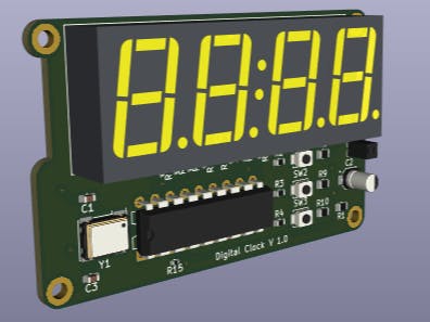
A digital clock is a type of clock that displays the time using numerals or digits, rather than using a dial and hands. These clocks typically use an electronic display, such as an LED or LCD screen, to show the time. Digital clocks are commonly found in devices such as radios, phones, computers, and standalone forms. They are often used because they are easily read and more accurate than analog clocks. Digital clocks can also display additional information, such as the date and temperature, in addition to the time.
In this project, we are going to look at how to design a simple standalone digital clock. We will look at the components required, the schematic diagram, how it works, and the PCB layout.
Components Used
1. 3, 10k resistors
2. 3, 820 resistors
3. 3, Push button switch (SW_SPST_B3U-1000P-B).
4. 1, PinSocket_1x02_P1.27mm_Vertical
5. 8, 100 resistors.
6. 1, PIC16F84A-041/P microcontroller.
7. 1, 220nF capacitor.
8. 2, 22pF capacitor.
9. 1, 4MHz crystal oscillator.
10. 1, CC56-12YWA display
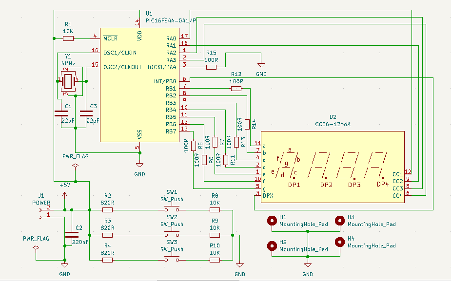
Circuit Diagram and How it worksThe system is designed around a PIC16F84A microcontroller with a 4MHz Crystal Oscillator and a CC56-12YWA display.
Generally, the digital clock typically uses the PIC16F84A microcontroller, to control the various components of the clock. This includes the display, which shows the time, as well as any other features the clock may have. The microcontroller receives input from a 4MHz clock crystal, which provides a stable and accurate time reference, and uses this information to control the display and other components of the clock.
The digital clock has push buttons in which you can set the time to adjust the hours, minutes, and seconds. The system works with low, 5V power.
PCB layoutA PCB layout is the arrangement of various components of a printed circuit board (PCB). The layout of the components on this PCB was done using KiCAD EDA and was carefully designed to ensure that the circuit functions properly and that the components are placed efficiently and compactly. This was done to prepare the system for production.
Gerber ViewsGerber files contain a graphical representation of the PCB layout, including the location and shape of the various components and conductive pathways on the board. These files are used by PCB manufacturers to produce the actual PCBs.
Below are Gerber’s Views of the PCB;
Below are 3-Dimensional render images of the PCB;
After coming up with a beautiful PCB project above and you are facing challenges implementing it, don't get worried. Several sponsorships exist the world over and among them is the exclusive and lucrative sponsorship offered by PCBway. The PCBway Non-profit Engineering Projects Sponsorship is a non-complex program that allows engineering more so electronics students to achieve their dreams in the area of PCB project success.
Your cool project might be sponsored when you.
1. Describe your team and project with appealing words and pictures as detailed as possible.
2. Upload your PCB files to our online quote system for placing your order.
3. Get a coupon after your article passes our audit.
4. Share our sponsor page to get more coupons.
To apply just click the application and it will lead you to the application page.


Comments
Please log in or sign up to comment.