The objective is simple! Build a harness that can help make contact with the debug pads on the ESP-8685-WROOM-03 module to program the module. Following is. visualisation of the position of the debug pads on the module.
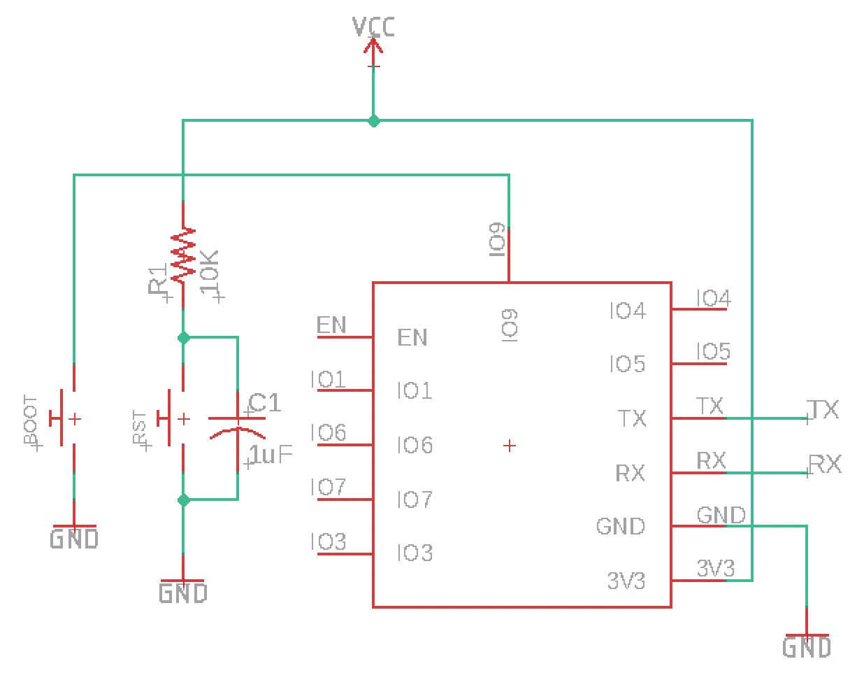
The basic circuit to program the module is the following. GPIO pin IO9 has a weak internal pull up. To put the module in programming mode IO9 is pulled low and the module is rebooted by connecting the EN pin to ground and back to its default high.
While programming this module I used spring loaded pogo connectors to make contact with the debug pads - 3V3, GND, TX, RX, IO9 and EN. The TX and RX pins to into a USB to UART module's RX and TX pin respectively and connected to a PC or Mac with Arduino IDE installed.
The connectors comprise of a probe with a spring loaded tip -
And a receptacle which has a lead to connect a female JST connector and to hold the probe on the other end -
When joined together they look like below -
What I then needed is to strategically position the pogo pins on the debug pads -
When assembled together the 3D enclosure looks as below -
The 3D printed pogo pin holder looks as below -
The ESP8685 module can be placed on the lower part of the 3D printed box with debug pads facing upwards and the top with the cover can be placed to make contact with the debug pads.
I used Prusa Mini+ to print the parts with 0.2 mm Quality settings. This resulted in a certain grit on the surface which made the parts to come together and remain enclosed -
I used the following settings on Arduino IDE -
The programming can be executed as ESP32C3 Dev Module as ESP8685 is comparable with ESP32C3 chip. Notice the Upload Speed set to 115200 to make the upload error free. Depending on the length of the JST wires even lower speed can be selected.
And that's pretty much it! Have fun programming with this jig if you build one :)


_3u05Tpwasz.png?auto=compress%2Cformat&w=40&h=40&fit=fillmax&bg=fff&dpr=2)
Comments
Please log in or sign up to comment.