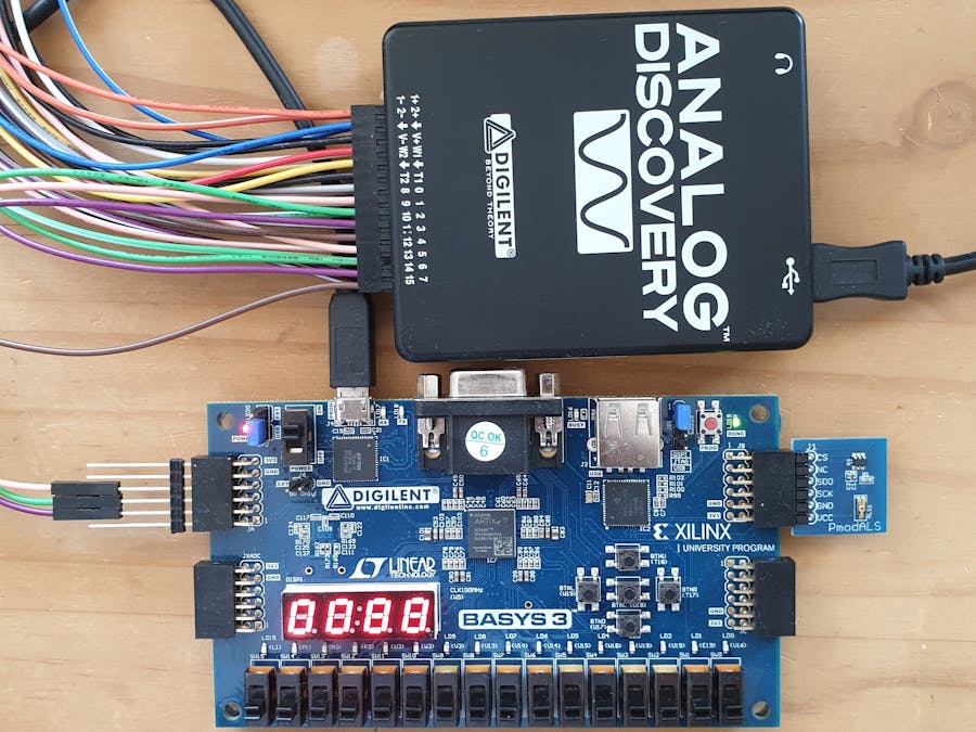
In this project, SPI Interface code is written in Verilog to interface an 8-bit ADC from Pmod-ALS. The 8-bit binary is converted to BCD and displayed on 7-segment display. The verilog code is synthesized on Artix-7 FPGA from Basys 3 board.
About me.. I have started to learn Verilog and it is very fulfilling and super exciting to think in terms of hardware. The project needs changes and improvements and I would be very happy to know what you think about it.
OverviewThe project is comprised of three modules as shown below.
- spi_interface
- double_dabble
- seven_segment_display
(Module: spi_interface)
Pmod Ambient Light Sensor (ALS) has an 8-bit ADC with a high speed SPI interface (ADC081S021 from Texas Instruments).
As debugging the timing on the hardware is extremely important, I have allocated 3 I/Os for monitoring the CS, SCLK, SDO lines of Pmod ALS on the Digilent Analog Discovery.
Note: Even though the timing is analyzed and debugged in Simulation (via testbench code), it became extremely needful to hookup some signals on the logic analyzer- indicated in blue boxes in the below figure.
The sensor specification depicts the following timing diagram, which is the complete basis for the verilog spi_interface code.
This is realized by two 8-bit counters and one 8-bit register.
reg [7:0] data_counter;         // Free running counter till 20, to time CS
reg [7:0] clk_div;              // Prescaler 100 MHz FPGA clock to 1.92 MHz SPI Clock
reg [7:0] r_RX_Byte = 8'b0000_0000; // MISO: Received 1 byte of data from PMOD_ALSClock divider (clk_div): From the main clock (100 MHz on Basys 3 board), derive spi clock (1.92 MHz).
The ADC on Pmod ALS converts analog values of light intensity into digital values which is then serialized to be transmitted on a SPI bus.
The first 3 bits and last 4 bits are zeros, and 1 tristate bit. The in-between 8- bits is data. Our verilog code captures this data synchronously with the help of spi clock.
Data counter: The data_counter is a free running counter which is clocked from spi clock. It is tuned to trigger data read and control chip select from/to the Pmod- SDO.
Once the data_counter turns 20, it is reset to 0. At 16, CS is pulled high as demanded by the timing diagram.
Note: CS could be made as input to this module so that a top layer application could command CS pin.
SDO dataread: Read SDO data into an 8-bit register (MSB first) as per the timing diagram Fig 6.
The read 8-bit data is converted to three 4-bit BCD vectors, to be able to drive each led at every decimal digit on the 7 segment display. Please read this beautiful article from Russel at https://www.nandland.com/vhdl/modules/double-dabble.html
I used his double dabble algorithm's verilog code and incorporated in this project. Thank you Russel :)
This module converts 4 bit BCD vectors to drive the leds of four seven segment displays on Basys 3 board.
Please refer Basys 3 Reference Manual for details on seven segment display. https://reference.digilentinc.com/programmable-logic/basys-3/reference-manual
Simulation:Please find the testbench code in the GitHub repo.
All the three modules are instantiated.
Serial data is transmitted on the SDO line for simulation and verification. It is to be verified that double dabble algorithm and anode/cathode control of seven segment display re working correctly.
Results:It was super fun working with this project. There are improvements needed to transmit the data byte at a reduced frequency and also in the seven segment display module, so that all the three digits from the data byte are displayed clearly on the display. I would be very happy to hear your thoughts on this project.
Most importantly special thanks to Russel from nandland.com and Greidi Ajalik from Simply Embedded. I am learning a lot from you and appreciate the work you do.
Thanks for the read!


Comments
Please log in or sign up to comment.