


Hardware components | ||||||
 |
| × | 1 | |||
Software apps and online services | ||||||
| ||||||
This tutorial shows how to do an HW design and code a SW application to make use of AMD Xilinx Zynq-7000 XADC. We will also see how to use the DMA to transfer data from the XADC into Zynq CPU's memory and stream data to a remote PC over the network.
This is the second of the three parts of the tutorial. In this part, I provide step by step guide for doing the HW design in AMD Xilinx Vivado.
The first part covered the XADC's concepts, and the third part will cover the SW application.
In this tutorial, I'm using the Digilent board Cora Z7-07S. However, all the principles described here can be used on any other Zynq-7000 board. I will highlight aspects specific to Cora Z7 in the text.
The Cora Z7 is a suitable board for testing the Zynq XADC because it has analog inputs that are usable in a practical way.
I'm using Vivado 2024.1.1 in this tutorial. Nevertheless, the same steps also work in Vivado 2023.1. My GitHub repository provides project exports for both Vivado versions.
Hardware design in VivadoMake sure you have Digilent board files installed. This article provides instructions on how to install them.
- In short: Download the most recent Master Branch ZIP Archive, open it, and extract the content of folder \vivado-boards-master\new\board_files into c:\Xilinx\Vivado\2024.1\data\boards\board_files\. You may need to create the folder board_files at the destination.
Create a new RTL Project in Vivado 2024.1. Select your version of Cora Z7 from the list of boards.
Let's first set the constraints.
Download the Cora-Z7-07S-Master.xdc from the Digilent XDC repository and import it in Vivado as a constraints file (this file will also work for Cora Z7-10).
We will use the two buttons, the dedicated analog input v_p/v_n (labeled V_P/V_N on the board) and the auxiliary input vaux1_p/vaux1_n (labeled A0 on the board; the vaux1_n is connected to ground, it doesn't have a pin on the board).
Uncomment the following lines in the constraints file:
## Buttons
set_property -dict {PACKAGE_PIN D20 IOSTANDARD LVCMOS33} [get_ports { btn[0] }];
set_property -dict {PACKAGE_PIN D19 IOSTANDARD LVCMOS33} [get_ports { btn[1] }];

## Dedicated Analog Inputs
set_property -dict {PACKAGE_PIN K9  IOSTANDARD LVCMOS33} [get_ports { Vp_Vn_0_v_p }];
set_property -dict {PACKAGE_PIN L10 IOSTANDARD LVCMOS33} [get_ports { Vp_Vn_0_v_n }];

## ChipKit Outer Analog Header - as Single-Ended Analog Inputs
## WARNING: Do not use both sets of constraints at the same time!
set_property -dict {PACKAGE_PIN E17 IOSTANDARD LVCMOS33} [get_ports { Vaux1_0_v_p }];
set_property -dict {PACKAGE_PIN D18 IOSTANDARD LVCMOS33} [get_ports { Vaux1_0_v_n }];
Specifying constraints for the dedicated analog input channel VP/VN is optional. Vivado will do synthesis and implementation even without the constraints specified.
For auxiliary channels, the constraints specification can be omitted only if you don't use other Zynq pins from Bank 35.
In our case, we need buttons and they are connected to pins in Bank 35 on Cora Z7. Without the constraints for VAUX[1], the implementation would fail because of incompatible IO standards error.
Create the block design.
Add the ZYNQ7 Processing System to the diagram. Vivado offers to run the block automation. Run it. DDR and FIXED_IO signals will be connected to the Zynq PS.
We need to configure the Zynq PS to meet our needs.
Enable Slave AXI High-Performance interface 0. This is the interface to which AXI DMA will be connected.
We will need 28 EMIO GPIO pins. Let's enable them in the Zynq PS configuration.
Note: After you close the Zynq PS configuration, Vivado will probably display a critical warning about negative DQS skew values. This warning can be ignored. I guess this is some glitch in the Cora Z7 board file. It has no negative effect.
There are 64 EMIO GPIO pins on Zynq-7000. The first 32 pins are in Bank 2 (EMIO pin numbers 54 through 85). Let me explain how we will use the first 28 GPIO pins from Bank 2 in our design.
EMIO pin number 54
Usage: output from Zynq PS; start input signal to the stream_tlaster.v (see the explanation in the DMA chapter)
EMIO pins number 55-80
Usage: output from Zynq PS; 25-bit value of the count input signal to the stream_tlaster.v (see the explanation in the DMA chapter)
EMIO pin number 81
Usage: input to Zynq PS; connected to the board's button BTN0
EMIO pin number 82
Usage: input to Zynq PS; connected to the board's button BTN1
Let's connect the buttons.
Create input port btn[1:0].
Since the buttons are the two most significant bits in the vector of GPIO signals, we need to concatenate them with a 26-bit zero value before we can connect them to the Zynq PS.
Add a 26-bit Constant with zero value to the diagram.
Add Concat to the diagram. Connect the constant to Concat's In0 and btn[1:0] to In1. Then, connect the dout of the Concat to GPIO_I of the Zynq PS. We now have the following diagram. (Don't be alarmed that Concat doesn't show the correct widths of the signals. Vivado will update this later.)
Now, we add a Clocking Wizard. It will generate the XADC input clock DCLK, i.e., the clock for AXI interfaces connected to the XADC, because, in our setup, the DCLK will be driven by the AXI clock.
Add a Clocking Wizzard to the diagram and connect clk_in1 to the FCLK_CLK0 output clock of the Zynq PS.
Change the source of the input clock from "Single ended clock capable pin" to "No buffer".
The "clock capable pin" setting applies to clock signals from an external pin, which the FCLK_CLK0 is not. Therefore, an input buffer (IBUF) on Clocking Wizzard is unnecessary. Leaving the source set as a "clock capable pin" may result in a critical warning during implementation on some boards.
Set the frequency of clk_out1 to 104 MHz. This frequency will allow us to run the XADC at 1 Msps. We will use a clock divider equal to 4, which gives ADCCLK of 26 MHz, which translates to the sampling rate of 1 Msps. See detailed explanation in the chapter Clocking, sampling rate, and bandwidth.
If you later want to experiment with slower XADC sampling rates, you can set the Clocing Wizard's output frequency and the clock divider differently so you achieve the desired sampling rate.
Set the Reset Type of the Clocking Wizzard to Active Low. This is because the FCLK_RESET0_N reset signal of the Zynq PS is active low.
Connect the reset signal of the Clocking Wizard with the FCLK_RESET0_N of the Zynq PS.
It's time for the XADC Wizard now. Add it to the diagram and open its configuration.
We will control the XADC from PS using functions from xsysmon.h. Therefore, we will only do a bare minimum configuration of the XADC Wizard in Vivado.
On the Basic tab, enable Enable AXI4Stream. We need the XADC Wizard to provide an AXI-Stream interface because this is how we get data into the RAM by means of AXI DMA.
In the Startup Channel Selection, select Single Channel (if not selected already by default). Then go to the Single Channel tab and select "VAUXP1 VAUXN1" (i.e., the auxiliary channel 1).
Notice that the XADC Wizard now exposes both VP/VN and VAUX[1] channels as input signals (VP/VN is always available as the input signal in all XADC Wizard configurations.)
That's all the XADC Wizard configuration we need to do.
Tip:
If you need to switch Single Channel mode between multiple auxiliary channels, follow this "hack" to expose them as input signals on the XADC Wizard:
Select Channel Sequencer in the Startup Channel Selection. Channel Sequencer tab will appear, where you can select as many auxiliary channels as you wish. It doesn't matter that you configured the XADC Wizard IP for Channel Sequencer mode. You will switch it to the Single Channel mode during runtime by calling XSysMon_SetSingleChParams().
We need to connect the analog channels.
Right-click on the Vp_Vn input signal of the XADC Wizard and select Make External. Repeat the same for input signal Vaux1. This will create two analog differential input ports in the diagram. The ports in the constraint file are properly named to match the ports we just created.
Vivado now offers Run Connection Automation. Run it.
Set all clock sources to the Clocking Wizard (/clk_wiz_0/clk_out1). As explained earlier, we want to drive the XADC clock from the Clocking Wizard to have the flexibility of choosing the frequency.
The Connection Automation added AXI Interconnect to connect the Zynq PS with the XADC Wizard. A processor System Reset was added to generate a reset signal for the AXI bus. Everything is clocked by the Clocking Wizard.
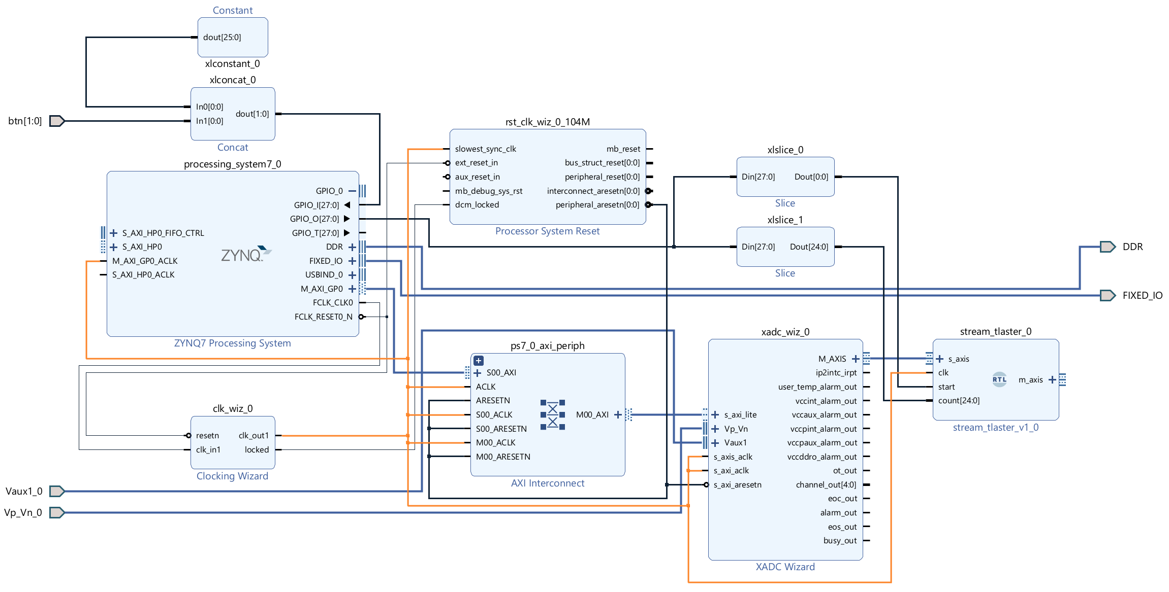
We now have the following diagram (I shuffled and rotated the IPs for better clarity).
As explained in the DMA chapter, we need to have the module stream_tlaster.v between the XADC Wizard and AXI DMA, and we need to connect its input signals to Zynq PS GPIO.
Add the stream_tlaster.v as a design source to the project. Add the module to the block diagram.
Connect the module's s_axis interface to the M_AXIS interface of the XADC Wizard. Connect the module's input clock (clk) to the output clock of the Clocking Wizard.
In order to connect the module's input signals start and count, we need to slice the 28-bit PS GPIO signal accordingly.
Add Slice twice to the diagram and connect both to the GPIO_O[27:0] of the Zynq PS.
Configure xlslice_0 to extract the least significant bit and connect its output to the start signal of the stream_tlaster module.
Configure xlslice_1 to extract bits [25:1] and connect its output to the count signal of the stream_tlaster module.
Our diagram now looks as follows (the image in full resolution is available here).
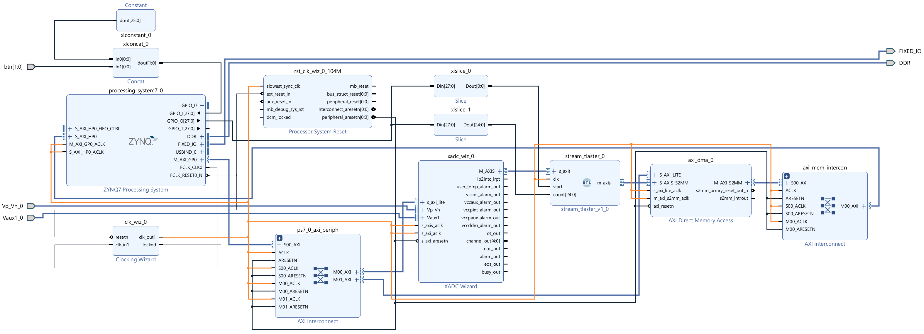
Now, add the AXI Direct Memory Access to the diagram and open its configuration.
We do not need to use AXI DMA Scatter/Gather Mode, so we disable the Enable Scatter Gather Engine option.
We set the Width of the Buffer Length Register to the value 26 (i.e., the maximum). This will allow us to transfer up to 33.5 million XADC data samples in one transfer (64 MB of data).
We are only writing to RAM, so we disable the option Enable Read Channel.
We enable the Allow Unaligned Transfer option on the Write Channel and increase the Max Burst Size to 128.
Connect S_AXIS_S2MM of AXI DMA with the m_axis of the stream_tlaster module.
Run Connection Automation, which Vivado offers now. Make sure to set all clock sources to the Clocking Wizard (/clk_wiz_0/clk_out1).
The automation connected the AXI DMA AXI-Lite interface to the Zynq PS via the existing AXI Interconnect. It created a new AXI Interconnect and used it to connect the DMA AXI master interface to the S_AXI_HP0 of Zynq PS. Also, the resets and clocks were connected accordingly.
We now have the final diagram (the image in full resolution is available here).
To make sure that nothing was missed, click the Validate Design button in the toolbar of the diagram window (or press F6).
You will probably see a critical warning about negative DQS skew values. This warning can be ignored. I guess this is some glitch in the Cora Z7 board file. It has no negative effect.
HDL Wrapper for the diagram needs to be created: Go to Sources|Design Sources, right-click on the block diagram's name, select "Create HDL Wrapper, " and select "Let Vivado manage wrapper."
Now, we create the design outputs: Click "Generate Bitstream" in the Flow Navigator on the left. Synthesis and Implementation will be run automatically before bitstream generation. There should be no errors.
Last but not least, we need to export the hardware specification to an XSA file. Go to File|Export|Export Hardware, and select "Include Bitstream".
Project filesThe repository's folder project_files provides the following files:
XADC_tutorial_hw_2024.1.1.xpr.zip
- Contains the HW design project export from Vivado 2024.1.1.
- This is the HW design for the Digilent Cora Z7-07S board, which we created in this article.
- To use the export, simply extract the.zip into a folder and open XADC_tutorial_hw.xpr in Vivado 2024.1.1.
- The archive contains exported HW, the file system_wrapper.xsa, which can be directly used in Vitis 2024.1.1 for creating the platform.
- Note: To have Vivado version 2024.1.1, you must install "Vivado™ Edition Update 1 - 2024.1 Product Update" on top of "Vivado™ Edition - 2024.1 Full Product Installation". See the Xilinx download page.
XADC_tutorial_hw_2023.1.xpr.zip
- Contains the HW design project export from Vivado 2023.1.
- This is the HW design for the Digilent Cora Z7-07S board, created using the same steps as described in this article.
- To use the export, simply extract the.zip into a folder and open XADC_tutorial_hw2023.1.xpr in Vivado 2023.1.
- The archive contains exported HW, the file system_wrapper.xsa, which can be directly used in Vitis 2023.1 for creating the platform.
The next part (the last one) of this tutorial provides an explanation of a SW application that will run on the HW design we just created.


Comments
Please log in or sign up to comment.