With this project I set out to design and implement a fast and area efficient multiplier for the NIST P-256 curve on an FPGA. The multiplier is written in VHDL, synthesis and implementation targets the Varium C1100 Blockchain Accelerator Card.
BackgroundThe task in this category of the Adaptive Computing Challenge 2021 is to accelerate blockchain applications/technology. By focusing on the fundamental part of blockchain technology, elliptic curve cryptography, we can accelerate not just one, but the blockchain technology in general.
The performance of an Elliptic Curve Cryptography (ECC) algorithm (ex. ECDSA) is heavily dependent on the multiply operation. As such it is of interest to maximize the performance of the multiplier unit.
But why is ECDSA so heavily dependent on the multiply operation? One might ask.
By investigating the operations in ECC we might get an answer. Operations in ECC can be viewed in a hierarchy with 4 layers, illustrated in the following Figure 1 below.
From the bottom up it consist of Finite Field Operations, Elliptic Curve Addition and Doubling, Curve Point Multiplication and Application/Protocol. The operations in one layer are implemented and dependent on the operations in the layer below it. For example the ECDSA protocol, associated with the top layer, is implemented using many curve point multiplications, which is associated with the layer below, Curve Point Multiplication. A small performance increase in the multiply operation associated with the layer Finite Field Arithmetic can result in a much larger performance increase in, as in this example, the ECDSA protocol.
The NIST P-256 curve operates on a bitwidth of 256. A general rule in digital design is that critical path delay increase with an increase in bitwidth. This is necessarily not true for all designs, but it tends to hold. This is the case for both adders and multipliers in an FPGA. Therefor this project has been all about designing and implementing a fast and area efficient 256 bit wide multiplier.
Design AspectsWorking with 256 bit wide values are no joke, to do it with a reasonably high clock frequency is almost scary. Lets see what problems will arise.
First to note about multiplication in an FPGA is that there are special hardware multiplier blocks called DSP blocks in the FPGA, we want to use them. Multipliers can be realized with other logic, but this will require some resources and run terribly slow. The DSP blocks on the other hand are designed for this very purpose, to multiply. And to do it fast, reaching 700-800MHz! But, if we want to use them we are limited to a maximum bitwidth set by the DSP block. In the case of the Varium card which is of the Ultrascale+ architecture, the limit is 18 bits for first operand and 27 bits for the second. Far off from the two 256 bits operands we want to multiply. Luckily we can divide and conquer, or width other words, use the technique of long multiplication we learned in the early days of school. Greatly explained by Srinath [1]. Figure 2 is a picture from the work [1] illustrating the multiplication of operand X and Y to form the result Z. Note that X and Y are split in 3 parts, each part n bits wide.
This translates to 9 partial results which are then added together. Each partial result is n+n bits wide and shifted some integer steps n. The final result Z is 6*n bits wide.
Furthermore, we established that the DSP blocks have a limit of its operands of 18 bits and 27 bits respectively. This is called an asymmetric multiplier and often written as 18x27. If we want to use the technique in Figure 2 it requires that both operands are the same bitwidth. Meaning we can not use the full potential of the DSP blocks. But fear not! Srinath [1] has tweaked the technique in Figure 2 to come up with the technique in Figure 3, utilizing asymmetric DSP blocks.
Now the X and Y operands are split in parts with different bitwidth, n and m. Partial products can now be calculated with high clock frequency and also very area efficient, since we use DSP block. To complete the multiplication we need to shift and add these partial products, should be easy enough. We will only need a 512 bit wide adder running at a few hundred MHz frequency.
Lets talk addersThere are many adder designs to choose from and some more complex than others. Aspects that we should consider are speed, area, design complexity and latency. To compare adder designs on all of these aspects could take very long time, in the end we can make due with something that is good enough. Lets start with the least design complexity possible, the +-operator in VHDL. The performance of a few different bitwidths can be seen in Figure 4.
Not to satisfying... We will have to come up with something else.
After some research on the web I found a promising design, described in a paper from 2016 [2]. Although the work in [2] targets an older Virtex-6 FPGA, we will have to see how the performance is on a newer device. The paper describes the design in great detail, too much to go in to here. But the general idea is to break the carry-chain path of the adder, which tend to also be the critical path, into two parts. Furthermore, to not utilize anymore resources than a normal adder generated by the +-operator does.
After some time, actually a couple of weeks. studying the paper and working on implementation I got some promising results. Turns out that the placement of individual LUTs and FFs are crucial for performance and that the placement tool in Vivado is not up for the task. Relative location (RLOC) attributes are heavily used in the design to achieve good performance. The placement on the device really needs to match that of the floorplan in Figure 5. If RLOC is not used the maximum frequency is well below the results of the normal adder in Figure 4!
There is one parameter in the design that is architecture-dependent and requires to be determined. This parameter is defined as M and we are to find M_opt, the optimal M. This is done by varying M and when M = M_opt, the highest frequency (or lowest critical-path delay) is achieved. The approach is described in the paper and for the Virtex-6 architecture M_opt = 36. The same approach was done on the Varium C1100 card for bitwidths of 256 and 512. The results are shown in Figure 6.
We can see that M_opt is between 80-96. Note that the Y-axis is critical path delay and not frequency, lower is better. We now got a 512 bit wide adder which runs at ruffly 450MHz, great!
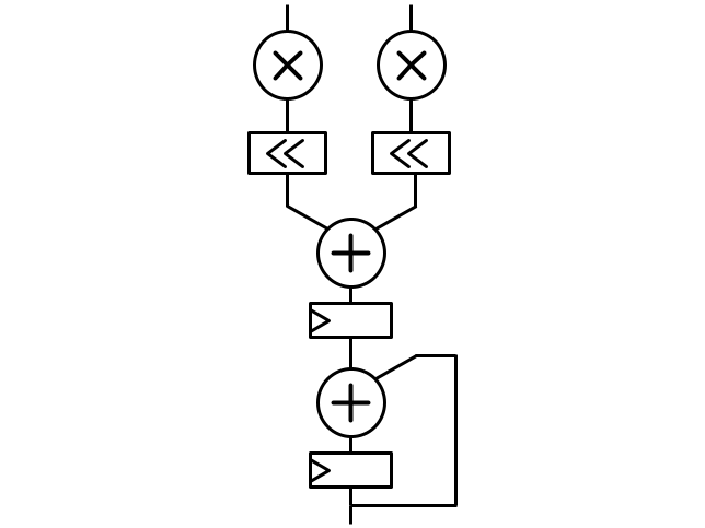
Multiplier designNow that we got the parts we just have to put it all together. As recalled from before, we need to multiply parts of the wide operands to get partial products, then we need to shift the partial products and lastly add them all. A full schematic of such a design is shown in Figure 7.
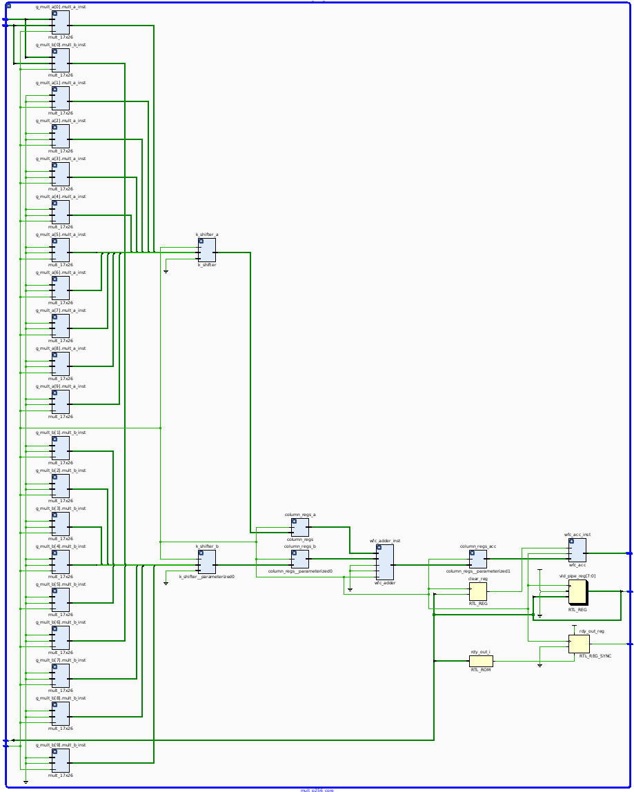
In Figure 7 we can see multipliers as a circle with a cross, shift-operation as a box with arrows, adder as a circle with plus sign and registers as a box with triangle. Although only 2 registers are shown in Figure 7, the multiplier has 5 registers in total. Extra registers are inserted in the shifter and also before the adders because of the strict requirement of floorplanning. The multiplier has a total latency of 21. This is due to the 5 registers, the DSP blocks having an internal latency of 3 cycles and that the multipliers needs to process 13 partial products each. Furthermore, what is not seen in Figure 7 is that the multipliers are comprised of 10 DSP blocks each. When utilizing the DSP blocks as a 17x26 multiplier we need 10 DSP blocks to fit the 256 bits wide values.
ResultsThe resource utilization of the design is listed below.
- 862 LUT
- 3092 FF
- 20 DSP block
The maximum frequency of the design is 372MHz, which translates to one multiplication in 56.5 ns or 17.7*10^6 multiplications per second.
Note that the pipeline is not considered here, next multiplication could be started as soon as the one before has cleared the first pipeline stage (multipliers).
ConclusionFirst I will note that the designed multiplier is not yet 100% complete, it is missing one minor functionality in one of the shifters and also the control logic is not yet implemented. This will lead to some increase in resource utilization, but will almost certainly have no effect on the maximum frequency.
A fast and area efficient multiplier has been design and implemented. Personally I think a higher frequency can be achieved, at the cost of an increased latency of 2.
The project/contest has been fun and learning. I realized mid way through the contest that my project goals where to high and optimistic, so I ended up changing the focus of the project. I want to thank both Hackster and AMD-Xilinx for making this possible.
See you in another contest!
Best regards William
References[1] Shreesha Srinath, Automatic generation of high-performance multipliers for FPGAs with asymmetric multiplier blocks, 2010.
[2] Petter Källström and Oscar Gustafsson, Fast and Area Efficient Adder for Wide Data in Recent Xilinx FPGAs, 2016.


Comments