Contents
1. Instruction
2. Development Environment
3. Data path Design
4. Control unit Design
5. Result
Instruction
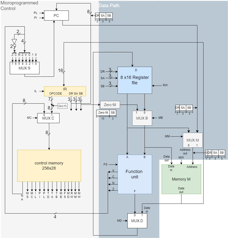
We designed the structure of the 16-bit CPU and built it into FPGA using Verilog HDL. It performs a program that receives 56 commands and sorts the data in the BRAM from small to large.
Development Environment
FPGA: Basys3 Artix-7
IDE: Vivado 2022.2
Data path
- Datapath
Data path consists of Register file, Function unit, and 3 Mux.
- Register file
Register file consists of 3to8Decoder, 8 Register, 2 8to1Mux.
- Function unit
It consists of ALU and Shifter.
- Shifter
We made 8 state (no shift, left shift, right shift, right rotate...) with barrel rotate method.
always@(*) begin
case(sel)
NO_SHIFT:  begin r_b = {i_b[14:0],i_b[15:0]};     r_num = 4'h0;  o_b = w_b_right; end
LE_SHIFT:  begin r_b = {i_b[15:0],15'b0};         r_num = 4'h1;  o_b = w_b_left;  end
RI_SHIFT:  begin r_b = {15'b0,i_b[15:0]};         r_num = 4'h1;  o_b = w_b_right; end
AR_SHIFT:  begin r_b = {{15{i_b[15]}},i_b[15:0]}; r_num = 4'h1;  o_b = w_b_right; end
LE_ROTATE: begin r_b = {i_b[15:0],i_b[15:1]};     r_num = 4'h1;  o_b = w_b_left;  end
RI_ROTATE: begin r_b = {i_b[14:0],i_b[15:0]};     r_num = 4'h1;  o_b = w_b_right; end
BR_ROTATE: begin r_b = {i_b[14:0],i_b[15:0]};     r_num = i_num; o_b = w_b_right; end
BL_ROTATE: begin r_b = {i_b[15:0],i_b[15:1]};     r_num = i_num; o_b = w_b_left;  end
default:   begin r_b = {i_b[14:0],i_b[15:0]};     r_num = 4'h0;  o_b = w_b_right; end
endcase
end
genvar i;
generate
for (i=0;i<BW;i=i+1) begin : br_gen_right
mux_unit inst_mux_unit_right (r_b[i+BW-1:i], r_num, w_b_right[i]);
end
endgenerate
generate
for (i=30;i>BW-2;i=i-1) begin : br_gen_left
mux_unit inst_mux_unit_left (r_b[i:i-(BW-1)], (BW-1)-r_num, w_b_left[i-(BW-1)]);
end
endgenerate
Control unit
- Control unit
It consists of PC,IR and control memory
Result
- Testbench Simulation
we can see that the data in the BRAM are sorted from the small values.
- FPGA Simulation
We can see Register0's outputs that sort data.


Comments
Please log in or sign up to comment.