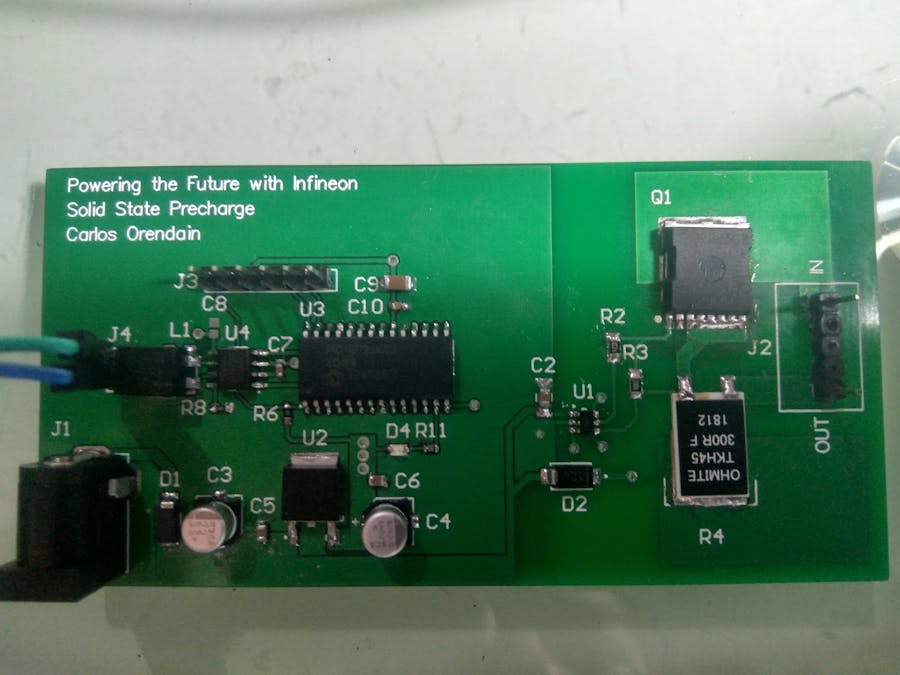
Right now all the electric vehicles use electromechanical relays or contactors for precharge function; this is expensive and not reliable. Using CoolMOS the cost will be lower and the physical size too, with better reliability.
Step One: Concept DesignThis webpage is a good start to know how to design a precharge circuit: http://liionbms.com/php/precharge.php
When initially connecting a battery to a load with capacitive input, there is an inrush of current as the load capacitance is charged up to the battery voltage. With large batteries (with a low source resistance) and powerful loads (with large capacitors across the input), the inrush current can easily peak 1000 A.A precharge circuit limits that inrush current, without limiting the operating current.
A precharge circuit between a battery and its load is required if any of the following are issues:
- The load has input capacitors will be damaged by the inrush current
- The main fuse will blow if asked to carry the inrush current
- The contactors, if present, will be damaged by the inrush current
- The battery cells are not rated for the inrush current
In the most basic form, the precharge circuit is operated as follows:
- Off: When the system is off, all relays / contactors are off
- Precharge: When the system is first turned on, K1 and K3 are turned on, to precharge the load, until the inrush current has subsided
- On: After precharge, contactor K2 is turned on (relay K1 may be turned off to save coil power)
In the solid state solution we're going to change K1 from Fig.1 with CoolMOS.
The Solid State Precharge system contains a microcontroller that generates a PWM signal of 1 KHz, PWM signal is connected to a High-Side Gate driver for control of the CoolMOS. This driver is capable to support up to 600V.
Additionally microcontroller has a CAN bus that will be connected to a main ECU of a vehicle; this make a possibility of externally control the precharge time.
In Fig. 4 there is a power jack (J1) with a polarity protection diode (D1). Also, a LDO regulator (U2) with his minimal circuit (C3, C4, C5 and C6), this regulator regulated the input voltage, 12V, to a lower voltage, 5V, for the microcontroller.
In Fig. 5 there is a microcontroller (U3) with a programmer port (J3) and his minimal circuit (C9, C10, R6, R11 and D4). The LED is for status, blinks when the precharge function is activated. The PWM signal (En_Precharge) generated by the microcontroller is the input of the gate driver. Additionally, there is a CAN bus for external communication.
In Fig. 6 there is the CAN transceiver (U4) that enables the external communication, also there is the minimal circuit (C7, C8, R8, R5, R7, L1, D3 and J4). A twisted pair is connected between J4 and the main ECU or a CAN to USB adapter for testing purpose.
In Fig. 7 there is the high-side driver (U1) with his minimal circuit (R9, R10, R1, C1, C2, D2), with this driver is possible to control the CoolMOS with a maximum voltage of 600V.
Also, there is the CoolMOS (Q1) with a series resistor (R2) to limit the gate current and a pull-down resistor (R3) to define a off-state as a default state. Connected to CoolMOS there is a series resistor (R4) on the source pin to limit the maximum current @600V to 2A. This resistor is capable of dissipate 45W, so the active time with 2A is minimal <1ms, this is not recommended. But with the PWM signal the power dissipated is less and is distributed on CoolMOS and R4. The load (DC-DC converter or Inverter) will be connect on J2.
Warning: Be careful when high voltage is present in the circuit.
Step Four: PCBThe schematic circuit was made on Circuit Maker, also the PCB layout.
After ordering a few PCBs and the components, it's time for coding.
Using Microchip MPLAB X IDE and MPLAB Code Configurator and some extra lines of code, is possible to control the activation of the CoolMOS.
In Fig. 10 there is the configuration of PWM5 peripheral of the microcontroller, is setted to 1 kHz at 50% duty cycle. This PWM is attached to the EN_Precharge signal.
Step Six: Assembly of PCBUnfortunately there is no photos of the assembly process. Duh!
After the assembly process, it's time for testing the Solid State Precharge.
The video shows the physical connection with an external power supply of 12V and a capacitor as a dummy load, the capacitor is rated to 450V with a capacitance of 330uF. Using a CAN to USB adapter is commanded the activation of precharge function. The capacitor's voltage is measured with an Analog Discovery 2.
In Fig. 12 is showed the result of precharge applied to a capacitor as a dummy load.
ConclusionThe Solid State Precharge was successful to charge a 330uF capacitor in 870ms with 24V. The time could be change with different PWM.
Unfortunately I was not able to make a test with a high voltage battery in the contest time; but it will be done in the future. Also some modifications, like a galvanic isolation of high voltage from low voltage and a diagnostic of the load's voltage, with the purpose of make a closed loop.


Comments
Please log in or sign up to comment.