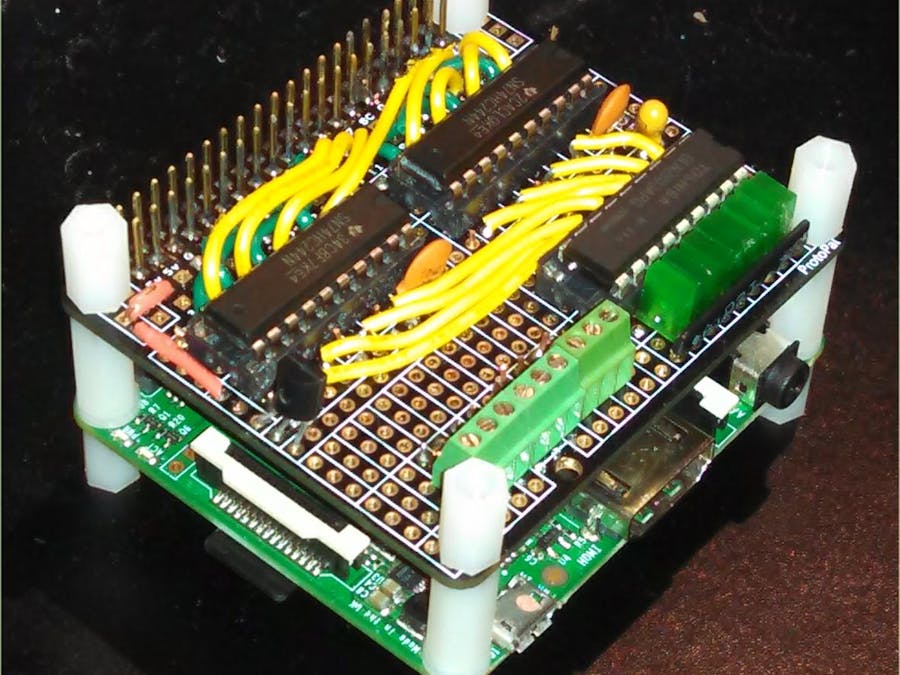
I needed 8 buffered inputs and 8 buffered outputs for a workshop controller. The computer would be a Raspberry Pi Model A+ and would have to stand alone. The entire project is at http://tigermountainsprings.net/project.htm.
This is a fun project. The wiring is difficult enough to be good training in soldering in small places. The wire paths can end up being your own personal design. After all a good electronics project is a work of art is its own genre.
ULN2803, socket
The project starts with the sockets for the SN74HC244N buffer ICs and the 3.3V regulator as suggested by The Cambridge Boffin Guide. The power supplied to this board is from the Raspberry Pi 5V supply. As the Boffin paper states, "It is better to have a 3.3 V voltage regulator on this board rather than use the 3.3 V from the raspberry PI GPIO pins. In case there was a short, it is much easier to replace this 22 pence regulator than the surface-mount device (SMD) regulator on the Pi."
The ULN2803A is only an 18 pin chip where the SN74HC244 is a 20 pin chip, however it is far cheaper to buy sockets in bulk so I am using a 20 pin socket for the ULN2803. As you can see in this image. Something will have to occupy the last set of pins so it isn’t confusing.
Pin-out logic
The Pin-Out logic of the 74HC244 makes it ideal for short wire jumpers with 4 inputs and 4 outputs wired to each chip from the Raspberry Pi connector’s side of the chip and the same on the opposite side.
Pin assignment
The Raspberry Pi A+ and B+ have a long list of GPIO however to use 8 inputs and 8 outputs means using 5 pins that are commonly used for other I/O. The ID_SD and ID_SC are forbidden and I2C should be available as well as the SPI. So the project uses 24, 26,35,38 and 40 (physical socket pins). These are used as outputs.
The project GPIO to socket wiring layout will be:
Power and ground
Most of the power and ground are wired on the bottom of the board. Note that more than one of the GPIO ground pins are jumpered to common ground. Losing a ground connection can be fatal to some devices and it is better to have redundancy in ground/common connection. The 5V is not yet wired to the ULN2803.
Pin numbering
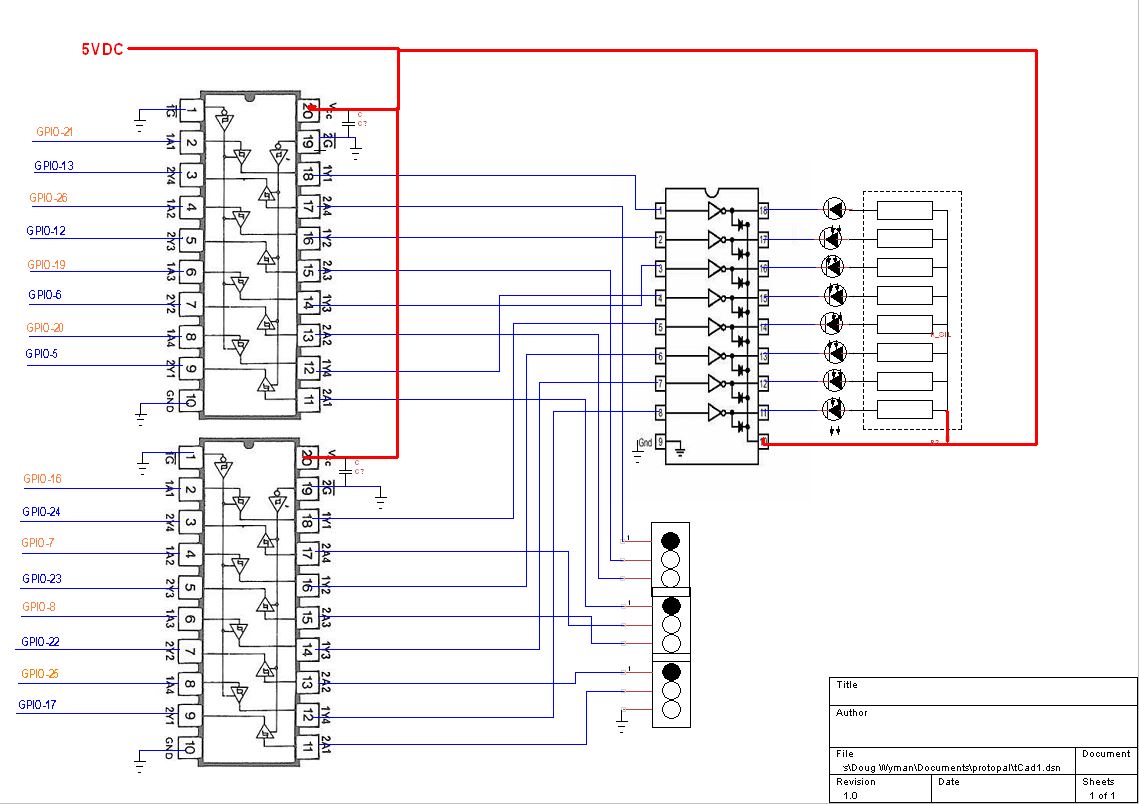
With the pins of the buffer chips wired, here is a project chart as a reminder which pin goes to which GPIO.
Top wiring
On the top now are the wires from the eight outputs (4 per chip) connecting the output buffer chip.
On the far side of that chip are a set LEDs connected through an SIP resistor array to 5v. Also on the top is a screw terminal block for the eight inputs.
Bottom wiring
On the bottom now are the wires from the eight inputs (4 per chip) connected to the screw terminals. Also the first of the 9 screw terminals is connected to ground.
You will note the addition of the GPIO connector.
Finished
Here is the finished project mounted on its Raspberry Pi A+. The outputs will be connected in a later project to a Pi Hat relay board through an eight pin connector but for now this has been a very fun project and if you have made it this far, thank you for looking while I play with my toys. Below is a snippet of Python test code:
import RPi.GPIO as GPIO
from time import sleep
GPIO.setmode(GPIO.BCM)

myInputs = [17,22,23,24,5,6,12,13]
myOutputs = [25,8,7,16,20,19,26,21]

for pin in myInputs:
    GPIO.setup(pin,GPIO.IN,pull_up_down=GPIO.PUD_DOWN)

for pin in myOutputs:
    GPIO.setup(pin,GPIO.OUT)

while True:
    for pin in myOutputs:
        GPIO.output(pin,True)
        sleep(.25)
        GPIO.output(pin,False)


Comments
Please log in or sign up to comment.