


Hardware components | ||||||
 |
| × | 1 | |||
Software apps and online services | ||||||
 |
| |||||
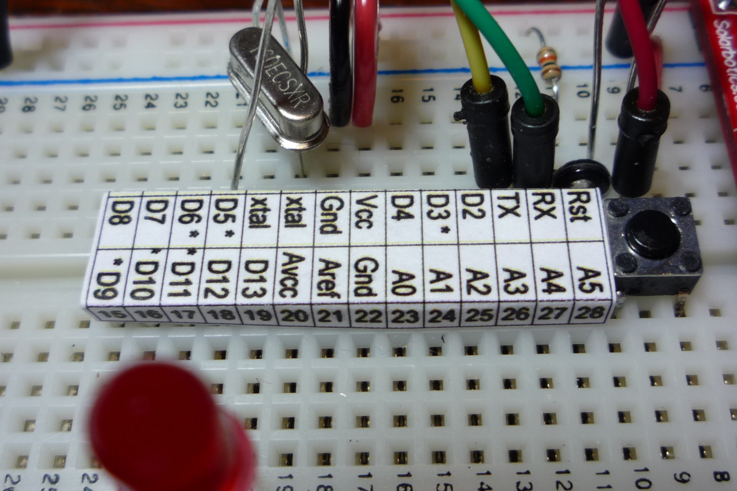
interface for breadboarding an Arduino, simple paper label that makes the translation of the pins simple.
ATMega168dnh.ods
ATMega168dnh.odsDownload
: Make a Spreadsheet
The first step was to create a spreadsheet. I used Open Office since it's available for Windows, Mac, and Linux and it's free for the downloading. Using Open Office, I created the spreadsheet ATMega168.ods.The cells have to be really small. The rows are 0.1 inch high to match the 0.1 inch spacing of the ATMega 168 pins. By trial and error, I found that the smallest font I could use was 6 point Arial Narrow, and the column widths are 0.12 inches for the pin numbers (columns A, D; F, I; and K, N), and the pin labels can be 0.18 inches wide (columns B, C; G, H; and L, M). Once I made one chart, I just duplicated the chart several times so I didn't have to use one sheet of paper to print out one tiny label.The asterisks by some of the pin labels, D3, D6, etc., indicate that these pins support pulse width modulation, PWM.To save you the time of creating the chart, the Open Office spreadsheet, ATMega168.ods is attached.
Print the Labels
I used a laser printer, but an ink jet should work just as well.Fold the labels for the legs of the chip before doing the final cut out. Those little labels for the pins are less that 1/8" wide and are hard to fold if the label has been cut to size before folding, but are easy if they are still connected.
Glue the Label on the Chip
In this photo, I pulled back the label "tent" so that you can see the chip under the label. To prevent the label tent from slipping I used a dab of rubber cement to hold the label in place. When you're done creating your prototype circuit, the label is easily peeled off the chip leaving no residue. The rubber cement doesn't melt the chip either.
The ATMega168 Label Is Complete
Prototype to your heart's content.
NEXTPCB PCB MANUFACTURER COMPANYNextPCB was founded in 2004 and has since established itself as a turnkey PCB manufacturing and assembly factory for prototype quantities as well as small-volume to big-volume production.
Why NEXTPCB?NextPCB provides one-stop services for PCB with professional PCB manufacturing practices fulfilling the advanced design requirements. The company provides the speed of PCB and assembly manufacturing with efficient collaboration and quality assurance.
NextPCB provides a variety of PCBs with optimistic capabilities. Starting from the single-layer they provide PCB services up to 20 layers, with a board thickness of 0.6mm to 2.5mm with a tolerance of 10% and much more capabilities. Check out the manufacturing capabilities of NextPCB for better production of your PCB.


Comments
Please log in or sign up to comment.