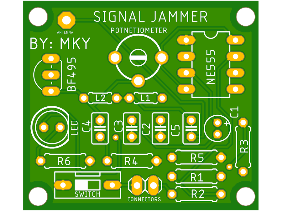
In this project, I am going to make a cell phone signal jammer PCB(Printed Circuit Board) using Autodesk Eagle which is used worldwide to design PCBs. In this Project First, we will make the schematic and then we move to the board layout and complete our design. In this project we are going to use NE555 Timer IC, Resistors, Capacitors both electrolytic and non-electrolytic, Inductors, a Trimmer, A Slide switch, A BJT(BF495), Antenna, a LED and Pin header for providing the power supply, you can use a DC Jack if you want to supply the board. The range of this signal jammer can be adjusted by adjusting the values of passive elements.
Open Eagle and create a new Project and go to the schematic.
Now after opening the schematic get all your components from the add parts option and connect them according to the schematic given below :
Make sure you make the connection perfectly as given in the schematic and add the correct name and value to each and every component. If you face any problem then you can check from the schematic file attached below. I recommend you make the same schematic as mine because it will be easier for you to place components on the board when we move to the board layout. Now you can run ERC(Electrical rule check ) to check whether there is any error in the schematic or not.
After completing the schematic click on the generate switch to board Icon to move to the board layout window and make sure to switch on the grid and size to 0.25mm and arrange all the components in a board of your desired shape and size.
Once you place all the components inside your board arrange them and start the routing process. This is a 2 LAYER PCB thus we make connections on both sides and make all the connections correctly. you can cross-verify with my design:
Make sure to apply a polygon and select the desired area. Add holes to the board of diameter 2.5mm in the above figure you can see all the red connections are from the top layer of the PCB and the blue ones are from the bottom layer to move one layer to another layer use VIA toll and make the connections. After that apply DRC(Design Rule Check) to check if there is any error or not. Then apply Ratsnest and you will get the top layer of your PCBs like this:
Now your design is finished and you can view your PCB by clicking on the manufacturing icon like this
You can change the color of the solder mask by clicking on manufacturing -> configuration setting-> solder mask color and choose the color you want for your PCB.
Here Are some of my favorite colors
I will Provide you with my Schematic and board layout in the attachment so that you can use it as a reference.
Here is the working video


_t9PF3orMPd.png?auto=compress%2Cformat&w=40&h=40&fit=fillmax&bg=fff&dpr=2)


Comments
Please log in or sign up to comment.