(This project is being managed here: Project Repository )
The mobile jammer is used to block the signals between the mobile phone and the base station. This can be done by generating some kind of hurdles for the range of frequency of signals. It will generate very low or no signals for the user. It has many applications like; for defense use, in educational institutes, and in offices during meetings. I have designed this mobile jammer for defense use. In military areas, they use mobile jammers to limit communication during hostage, bomb threats conditions, and military operations.
The benefit of using these jammers is to make secure everyone from any worst situation. Because in these cases the use of the mobile phone can be a source of communication between terrorists or opponents. I have designed the PCB board of mobile jammer that is very flexible to use as it is portable can be carried in the pocket by providing a user-friendly interface. Moreover, a proteus simulation of the design is also available to test its work. In the end, I have uploaded all the design files on the Inventhub for the manufacturer and the user.
Working Description:
The working mechanism of the mobile jammer is very simple to understand through the following block diagram.
The first step is to power the mobile jammer through the battery; it could be 9V. Then the oscillator circuit will generate an RF signal, this circuit consists of a transistor, two capacitors, and a resistor. This signal is made to a specified frequency and made randomly using a noise generator circuit. Then the amplifier will amplify the generated signal through the tuned circuit. This amplified signal will be sent to the antenna using a capacitor that will allow the AC signal to pass by blocking the DC signal. When the transistor will turn on the tuned circuit will also turn on. This will act as an oscillator and further can be used to produce a high frequency. All these stages will combine and transmit to the air and through this jammer circuit, mobile phone signals can be blocked easily.
Schematic Diagram:
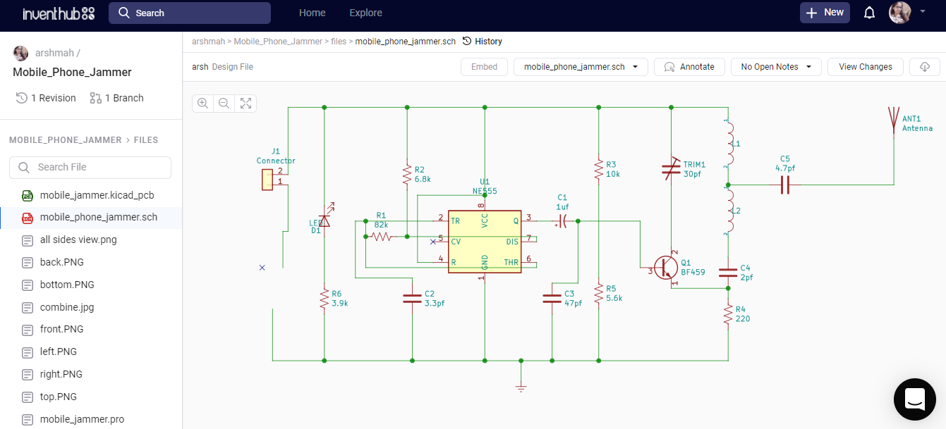
In the schematic design, the main component used is the NE555 timer, It is an IC that is used to generate frequency or signals. It has 8 pins; one control and one reset pin. This can be used in delay and oscillator applications.
The output of 555timer will be sent to the amplifier through a capacitor that will block the DC part of the signal and only allow the AC signal to pass. Then this signal will be amplified by the transistor and will be sent to the antenna.
I have uploaded all the schematics and 3d step files of the component online on Inventhub. For fabrication, I will send these files to the manufacturer he will make my design without any error on the board. This is the link to Inventhub where my design files are available.
PCB Board Design:
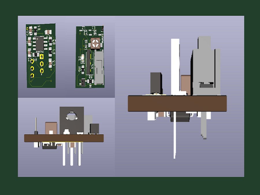
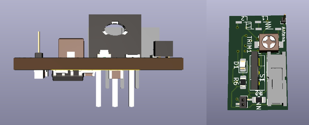
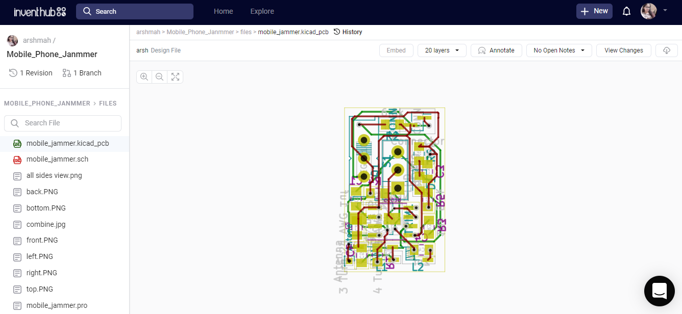
I have created the design of the PCB board with Double-layer PCB; it has a conductive layer of copper on both sides of the PCB board that is means we can embed components on both sides. Instead of connecting all the components on one side of PCB that will ultimately increase the size and cost of the design, I have implemented it on two sides that allow the components to connect and drill from both sides of the board. Hence, cost and size are reduced.
I have uploaded all PCB design files on Inventhub, the manufacturer can easily download the release file i.e. the zip folder containing all design files, and fabricate my PCB board. Inventhub is the link to the release file.
Proteus Simulation:
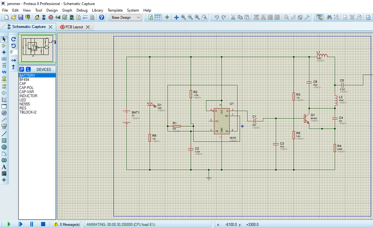
I have implemented the design on Proteus to observe the working of a mobile jammer. Here is the complete design. We have three major subcircuits here which are responsible to jam the signals of mobile phone
- RF amplifier (Transistor, capacitor, and resistor)
- Voltage Controlled Oscillator (the oscillator that can be controlled by voltages)
- Tuning circuit
Bill of Material:
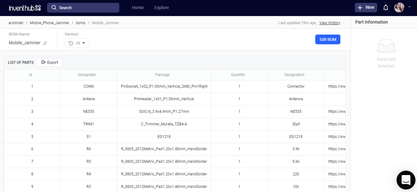
After the step of fabrication, I need to embed my components on the PCB board. Instead of visiting my component provider and telling him manually about the components that will enhance the chances of error, I will create a list of components with the exact size, dimensions, and library reference in Bill of Material on Inventhub. He will download the file and will deliver the components as per my design requirement.
Here you can find the BOM file at Inventhub.
Feel free to ask any query at arshmah@inventhub.io






Comments