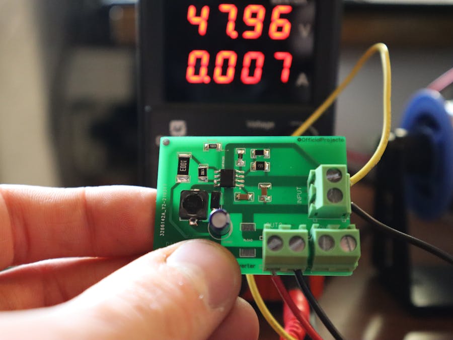
In electric vehicles, the potential difference across the battery pack is always much greater than the voltage at which the control logic boards work. Due to the need to have a low voltage power supply line, often equal to 5V, it is necessary to use special electronic circuits called “Step down converters”. Through these devices it is possible to convert the voltage very efficiently, in fact it is possible to reach values of η equal to 95%.
For the realization of the PCB I relied on JLCPCB, a leading company in the production of very high quality PCBs at truly competitive prices. Thanks to the use of EasyEda it was then easy to send the PCB into production, where you have a wide choice of parameters such as: color, size, electrical tests, gold pins, and much more! They also offer the possibility to mount the components to them on the PCB and send you the finished circuit!
Finally, they can also carry out RoHS tests and produce PCBs in large quantities, so that they can also meet the needs of companies.
Specifically, if you choose to produce only 5 PCBs, the price is $ 2!
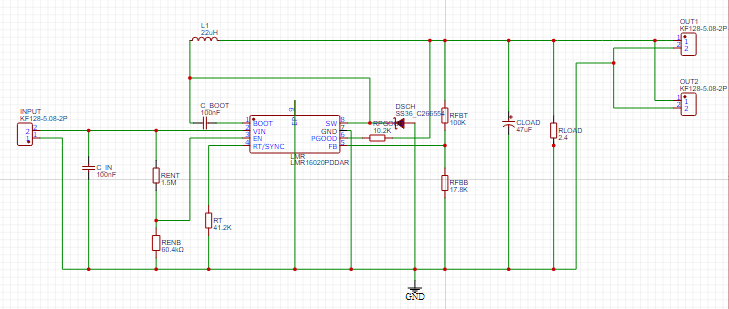
In the case in question, it was decided to develop a Buck Converter through the integrated LMR16020. The particularities of interest of this integrated are the following:
- 1. Input Voltage Range: 4, 3 V to 60 V. Considering to use a battery pack with a nominal voltage of 48V, the voltage range at which the step down converter works is suitable for coping with the voltages supplied by the battery
- 2. 2 A Continuous Output Current. Such an output current can provide power to multiple low-power devices at the same time, or to a single larger device such as the Nvidia Jetson Nano
- Integrated High-Side Mosfet. In this way it is possible to save space on the PCB and avoid the problem of choosing a suitable mosfet to make the circuit more efficient
- Ultra-low 40 μA OQC & Ultra-low 1 μA Current in Shutdown. The integrated has been designed to offer excellent performance in circuits where batteries are used. Thanks to these features it is also possible to save energy, extending the battery life
- Thermal, Overvoltage and Short Protection. Very important aspects that are not guaranteed on all "buck converter" ICs, it is possible to preserve the digital logic circuits in case of failure
The desired parameters, around which the buck converter was built are:
- Input voltage: V_IN 48V
- Output Voltage: V_OUT 5.0V
- Maximum Output Current: I_OUT 2.0 A
- I_EN 1 μA
- I_HY S 3.6 μA
- Transient Response 0.2 A to 2 A: 5%
- Output Voltage Ripple: 10mV
- Input Voltage Ripple: 400 mV
- Switching Frequency: f_SW 600 KHz
The output voltage delivered by the LMR16020 can be set as desired using a voltage divider consisting of a top feedback resistor R FBT and a bottom feedback resistor RFBB. The equation that relates the two resistors is the following:
RFBT = (V_OUT − 0.75)/0.75 × R F BB
Choosing a value of 100 kΩ for R_FBT, considering the V_OUT voltage equal to 5V, we obtain that R_FBB is about 17.65 kΩ. Rounding, it results 17.8 kΩ.
Switching FrequencyTo calculate the value of the resistance RT, able to set the working frequency, it is necessary to consider the following formula:
RT (kΩ) = 42904 × fSW (kHz)^(−1.088)
Considering a working frequency of 600 kHz, we obtain that the RT value is 40.72 kΩ. Consequently, the real value of a resistor closest to the theoretical one obtained is 41.2 kΩ.
Output Inductor ChoiceTo choose the value of the inductance it is necessary to consider some input parameters, but above all the maximum current ripple to be obtained. The larger the latter, the more the efficiency of the overall circuit deteriorates. As it grows as the input voltage increases, the minimum value of the LMIN inductor can be calculated using the maximum input voltage. Considering KIND as a coefficient that represents the amount of current ripple relative to the maximum output current, setting it to satisfactory results 20 % are obtained. The calculation of the inductor value continues as follows:
△iL = [V OUT × (V IN MAX − V_OUT )] / [V_IN_MAX × L × f_SW]
L MIN = (V_IN_MAX − V_OUT) / (I × K_IND) × (V_OUT) / (V_IN_MAX × f_SW)
In this case, the following parameters were chosen for the inductor calculation:
- V_IN_MAX: 48 V
- V_OUT: 5.0 V
- f_SW: 600 kHz
- K_IND: 20 %
The obtained LMIN minimum inductance value is 17.716 μH, subsequently choosing an inductor of 22.0 μH value for the real implementation. In this way, a ripple value of 0.400 A is obtained.
Output Capacitor ChoiceThe output capacitor of the step down converter takes care of managing the output voltage ripple when the converter is in steady state. this ripple at the output consists of two fundamental components: the first is a consequence of the ripple present at the output of the inductor that crosses the Equivalent Series Resistance (ESR) of the capacitor:
△V OUT = △iL × ESR = K_IND × I_OUT × ESR
The second contribution is caused by the ripple of the inductor which charges and discharges the capacitor:
△V_OUT_C = (△i_L) / (8 × f_SW × C_OUT) = (KIND × IOUT) / (8 × f_SW × C_OUT)
Since the two components are out of phase with each other, the overall output ripple is lower. To calculate the minimum value of the capacity, the following formulas are used, and then the greater value of the two obtained is taken:
COUT > 3 × (IOH − IOL) / (f_SW × V _US)
COUT > (I_OH^2 − I_OL^2) / [(V_OUT + V_OS)^2 − V_OUT^2] × L
Considering the following design parameters:
- KIND: 20 %
- IOL: 1.6 A
- IOH: 2.4 A
- △V_OUT_C: 10 mV
- V_US: 5% V OUT = 250 mV
- V_OS: 5% V OUT = 250 mV
we obtain that COUT cannot be less than 8.33 μF. Choosing as the minimum value, the maximum value obtained by calculating COUT from the last two equations shown, we obtain that it must be greater than 23.37 μF (against 16.0 μF ). For the physical realization a capacitor with a value of 47.0 μF was chosen.
Schottky Diode ChoiceThe breakdown voltage of the diode should be at least 25 % greater than the maximum input voltage. For greater reliability, the current supported by the diode must be at least equal to the maximum output current to the converter. In this case, a diode is chosen that can support a maximum of 2 A In any case, it is possible to consider a diode capable of supporting IOUT × (1 − D) [A], where D is the duty cycle of the converter switching signal.
Input Capacitor ChoiceFollowing the datasheet of the LMR16020 it is noted that a capacity is needed to filter the high frequencies. The use of capacitors ranging from 4.7 μF to 10 μF is recommended, but a 100 nF capacitor can also be used, and in fact the latter was chosen.
Bootstrap Capacitor ChoiceAlways following the datasheet of the LMR16020, a capacitor CBOOT is inserted, which plays the role of bootstrap capacitor, of the value of 100 nF and able to support at least a voltage of 16 V.
Step Down Converter SimulationFrom the simulation it is possible to first notice that the voltage reaches the desired value of 5 V. Subsequently, to arrive in steady state the circuit takes about 4.5 ms, which is sufficient for the type of application for which it will be used. It should be noted that the average value of the output current is not 2 A but is lower. In any case, the output current is sufficient to power the Jetson Nano as well. Finally, it can be observed that the ripple of the output voltage is extremely low, almost absent, while the ripple of the output current is quite important. Through physical tests of the device we will determine the overall quality of the circuit.
PCB Routing & Physical RealizationAn important aspect of the physical construction of the circuit are the dimensions: since the voltage converter must be physically positioned close to other electronic boards, the smaller it is, the more comfortable it is to insert. The routing was completely carried out on a single layer, thus avoiding having to create routes between the front and rear layers. The circuit will be connected to the battery via a 5mm DC connector, while it will be possible to connect to the output of the latter via screwdriver pins.
OLD VERSION
FINAL VERSION
At this link you can find the files relating to the current version of the PCB and the new one. Following various tests, it was necessary to improve the paths on the PCB. At the link you can find the gerber file, the BOM file and the pickandplace file
files: bit.ly/38gNRk9
Visit: https://jlcpcb.com


Comments
Please log in or sign up to comment.