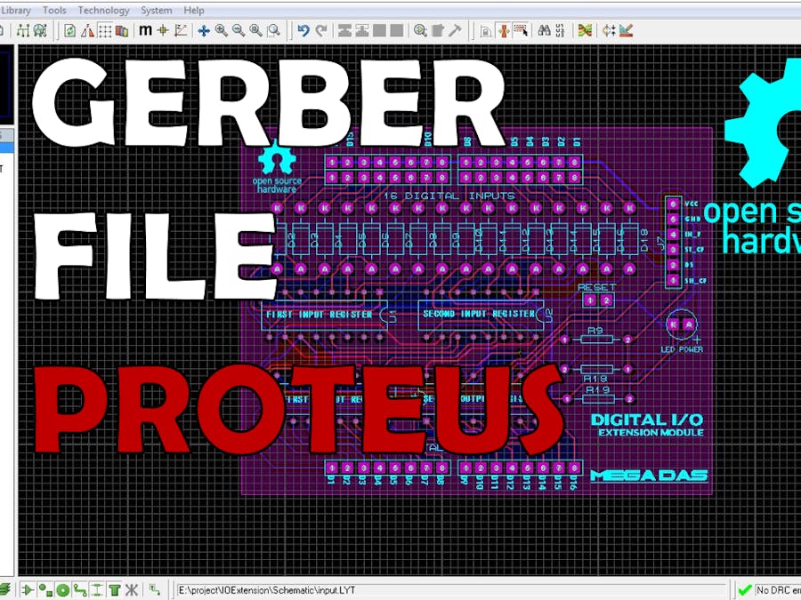
Talking about Gerber files, in most of my previous projects I was always advising you to create your own PCB design in order to introduce a better appearance for your project, and in many projects I was recommending the use of JLCPCB platform as a PCB supplier since it provides a great service with a cheapest cost and I was telling to upload your Gerber files in order to produce the PCB design that you have created for your project but what are these Gerber files in the first place!
Searching across the internet, The Gerber files or Gerber format is "an open 2D binary vector image file format". It is the standard file used by (PCB) industry software to describe the printed circuit board images like the copper layers, solder mask, legends, etc.”
From here we can notice that Gerber is used in PCB fabrication data. PCBs are designed first on a specialized electronic design automationor what we call (EDA) or a computer-aided design (CAD) system. The CAD systems output PCB fabrication data to allow fabrication of the board. This data typically contains a Gerber file for each image layer and we can find many files extensions depending on the layers of the design so we can find the ‘top copper file’ the ‘top soldermask file’ the ‘topsilk file’ etc and each one has its extension format.
Extension Layer
· pcbname.GTL Top Copper
· pcbname.GTS Top Soldermask
· pcbname.GTO Top Silkscreen
· pcbname.GBL Bottom copper
· pcbname.GBS Bottom Soldermask:
· pcbname.GBO Bottom Silkscreen:
· pcbname.TXT Drills
· pcbname.GML/GKO *Board Outline:
· 4 layer board also need
· pcbname.GL2 Inner Layer2
· pcbname.GL3 Inner Layer3
All the files are enclosed in one folder and compressed to a.rar or.zip archive with standard file extension: There are two major generations of Gerber format:
- · Extended Gerber, or RS-274X. This is the current Gerber format.
- · Standard Gerber, or RS-274-D. This obsolete format was revoked.
In order to get the Gerber files of the circuit design to produce the PCB we need a EDA or a CAD system, in this article I will use Proteus software to show you how to get Gerber files from a circuit design and then upload it and produce it using JLCPCB platform but if you are running another CAD system like Altium designer, circuit maker, eagle, Kicad etc you can refer to following article and select the EDA you are using and you will get assistance on how to get GERBER files.
So I will get back to one of my old projects which has a circuit board that could add more digital inputs and outputs for any Arduino board, I was using Shift registers in this project and some other electronic components to create the following schematic under Proteus ISIS
talking about the schematic, it will be much better if you make it clear from the beginning so avoid the use of many wires and use terminal connection to create a clear schematic.
Once I made the schematic I moved to Proteus ARES extension to design the appropriate PCB for my project, the circuit design has two layers and I have included some logos and labels in the top silk layer “remember its file format is GTO”.
Once you finish the circuit design you can get its Gerber files from Proteus ARES by clicking on OUTPUT then you select “generate Gerber or Excellon files"
Once you click on it, the CADCAM Output window will appear and you have to select some parameters:
So first you need to select the folder in where you want to save the.zip file
Select the option of output as zip file and just tick the other options
Moving to the layers and artworks section where you should select the layers that you have in your design, so in my case I’m using the top and bottom cooper since the design is a two layer design, top and bottom silk, top and bottom resist the edge file the mech1 file and the drill, well the drill file has a TXT extension and it indicates where to make the drill for each through-hole component lead
Select the millimeter unit and do not forget to select the RS274X format, then the last parameter is the resolution, a 500dpi is good for most machines.
Once you click ok you get your Gerber files ready.
Now if you want to place an order, just move to JLCPCB website where you can upload your circuit design using the saved Gerber files, before moving to the payment part, you can make one last check on your PCB design using the PCB viewer which display the final view of your PCB design.
You can watch this video for further details :


_4YUDWziWQ8.png?auto=compress%2Cformat&w=48&h=48&fit=fill&bg=ffffff)


_Ujn5WoVOOu.png?auto=compress%2Cformat&w=40&h=40&fit=fillmax&bg=fff&dpr=2)


Comments
Please log in or sign up to comment.