Washington State has set a goal to transition to zero-emission vehicles (ZEV) by 2035. However, current Electric Vehicle Supply Equipment (EVSE) charging systems suffer from compatibility issues, with a 30% chance of incompatibility between charging stations and electric vehicles. Our senior design project is to develop an open-source EVSE charger hardware platform that is reliable, efficient, and easy to implement, simplifying electric vehicle charging.
We partnered with PHYTEC to create an open-source reference design for EVSE, specifically implementing level 1 charging. The design leverages PHYTEC's phyCORE-AM62x System on Module (SOM), which is expanded onto two PCBA's: the digital board and the analog board.
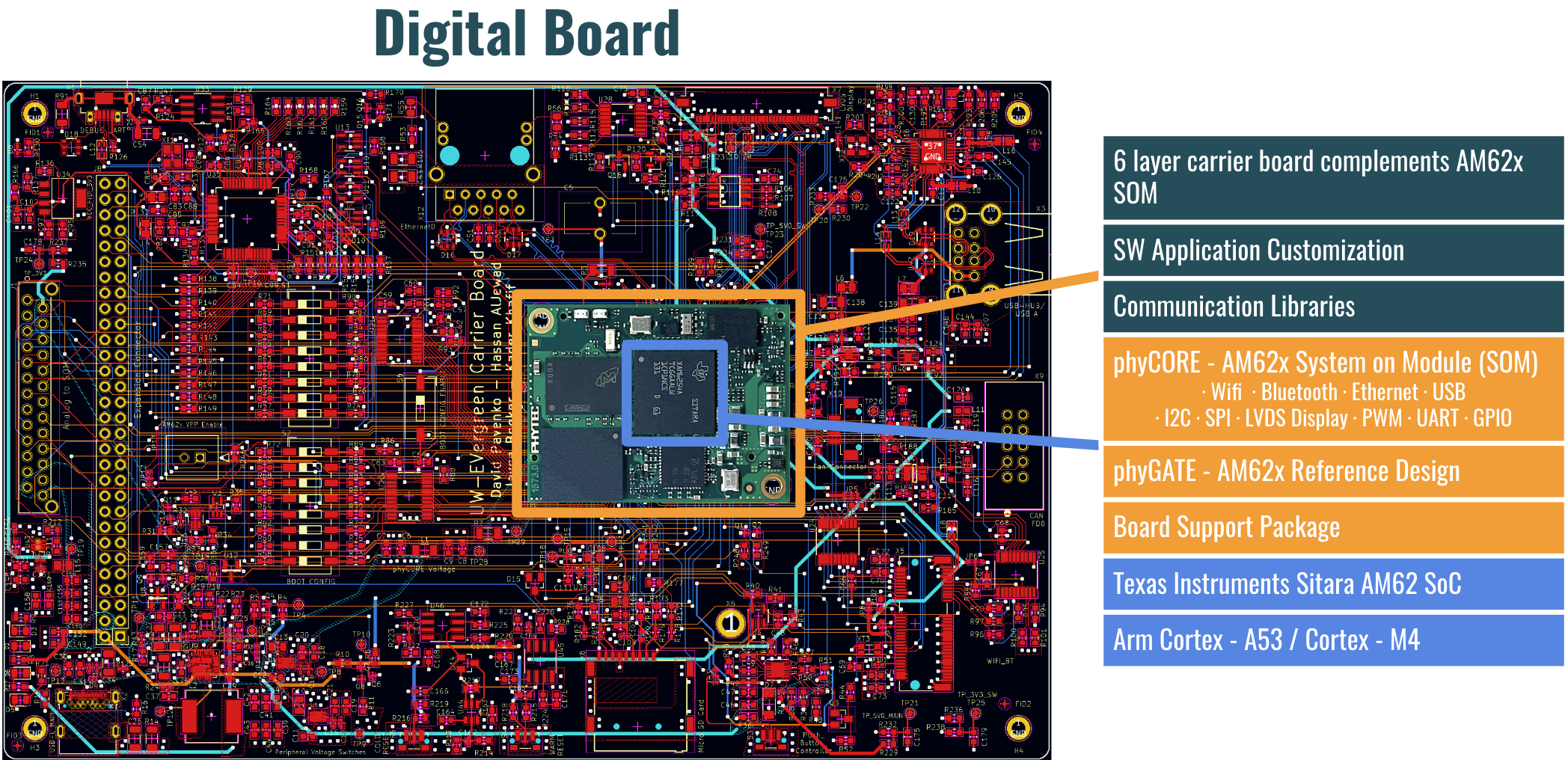
The digital board is a carrier board for the AM62x SOM that allows us to access the interfaces provided by the SOM. The digital board has a wide number of interfaces that utilize the AM62x SOM like LVDS Display, HDMI, Ethernet, CAN FDO, WiFi & Bluetooth, etc. The requirements for the SOM would be to generate the Control Pilot line which is a 1 KHz Pulse-Width-Modulation (PWM) that's used to provide bi-directional communications between the electric vehicle and charging system. The digital board is responsible for controlling the relay on the analog board that will deliver the power to the EV. The digital board will also monitor the charging procedure to ensure safe operation by monitoring Reverse-Current Detection (RCD) and Weld Detection on the relay.
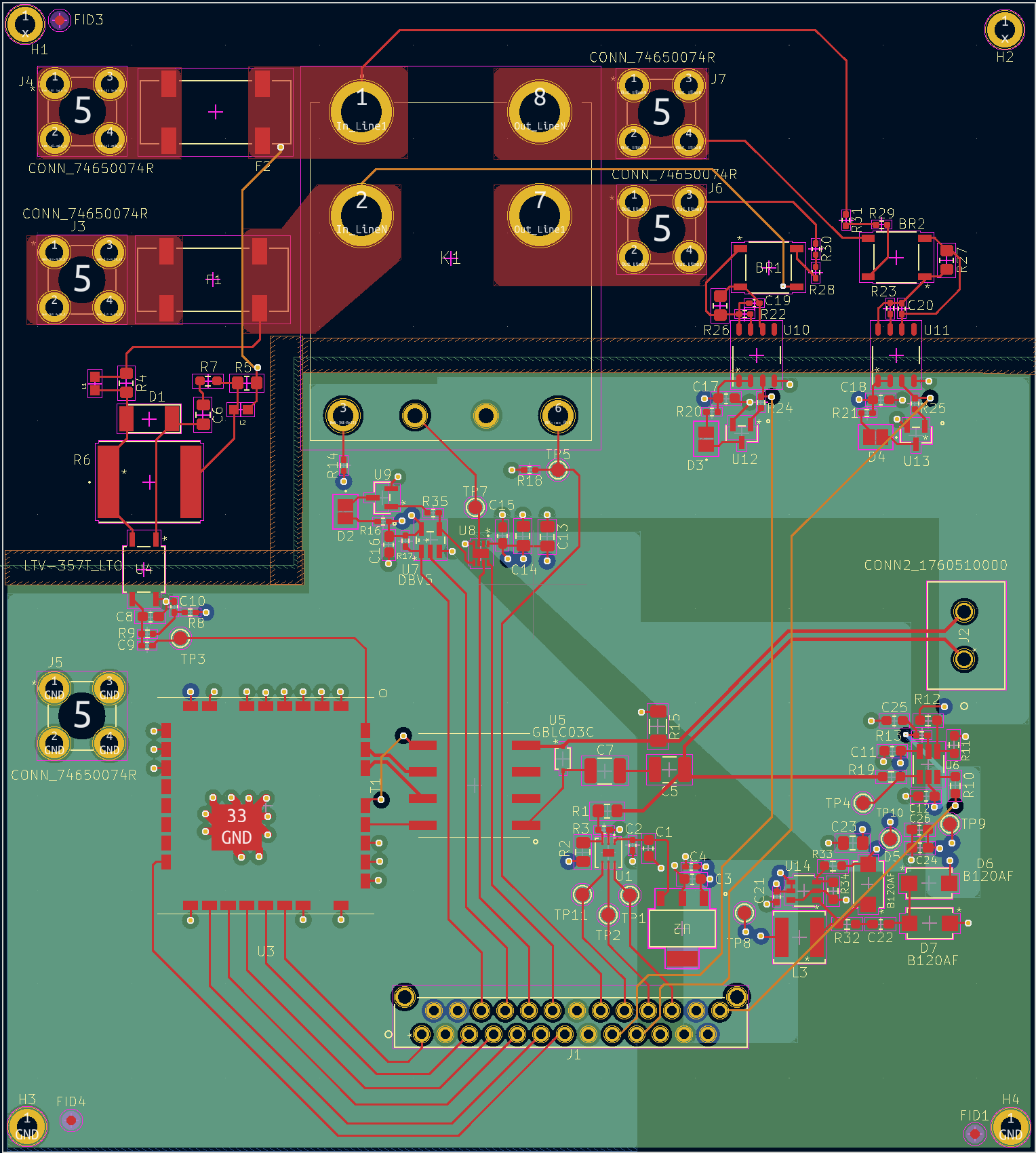
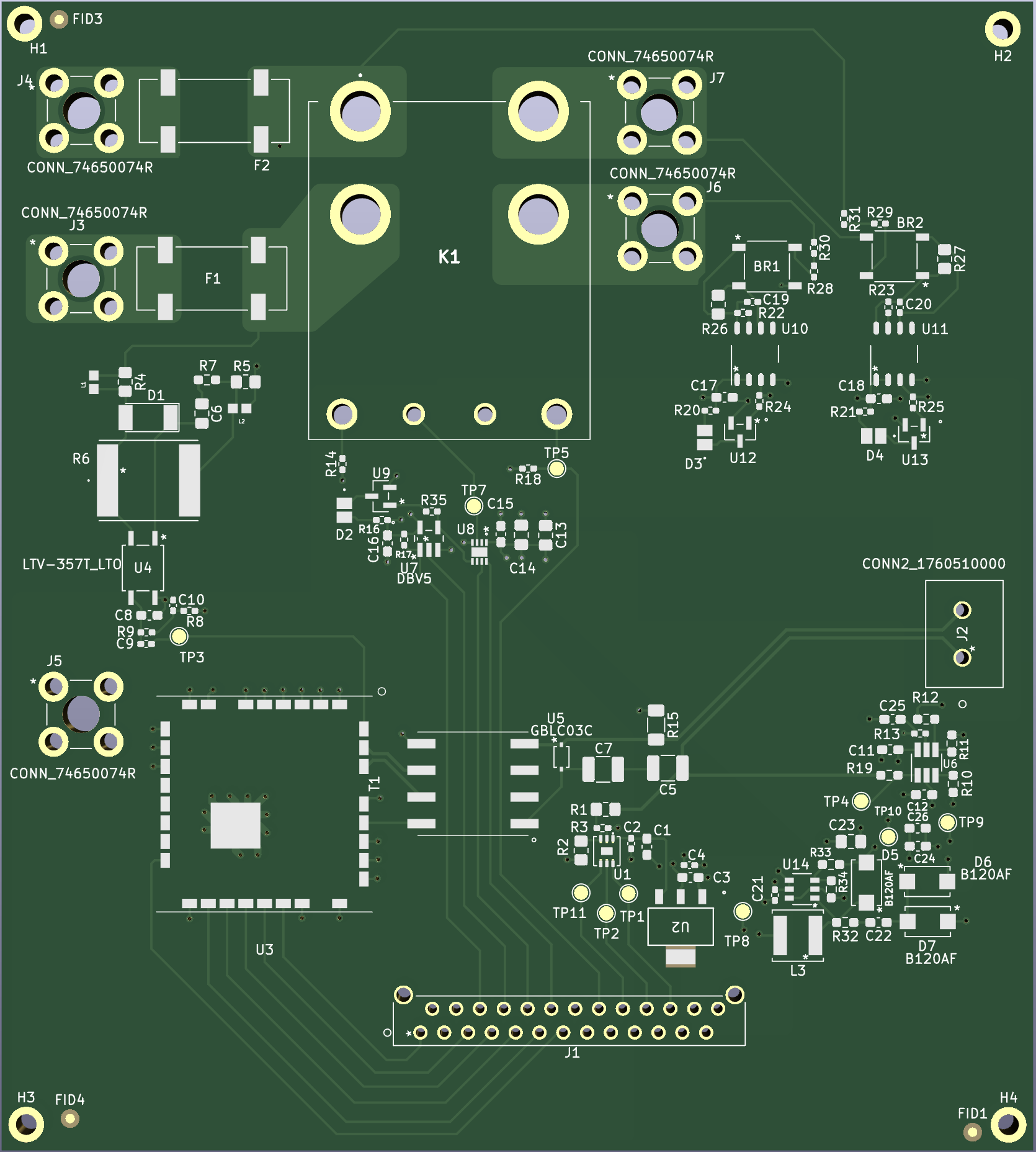
The analog board handles power delivery and protection. Since we are using Level 1 charging, the analog board will receive 120V AC line from the outlet and deliver that to the vehicle through the relay controlled by the digital board. The analog board will also house the RED BEET module, which is responsible for Vehicle2Grid (V2G) Integration.
The RED BEET module generates a 20MHz signal that's superposition on top of the CP Line. This signal will be used to authenticate the vehicle with the power grid and allow for payments. The system has another safety feature which is to make sure that the plug is connected to the vehicle, and not anything else. This will be done through the proximity pilot (PP) line which involves a switch on the adapter that changes the line impedance if connected to the vehicle.
To ensure compatibility and ease of implementation, an open-source Linux software and a board support package were developed, with a focus on customization and delivering a production-ready image via GitHub.
The successful implementation of our open-source EVSE design will lead to simple and efficient charging systems, enhancing the accessibility and reliability of EV charging stations. This will encourage more individuals to adopt electric vehicles. The project has the potential to democratize the development of EV charging infrastructure, promote the adoption of zero-emission vehicles, and significantly reduce carbon emissions, thereby improving air quality and combating climate change.
DesignThe project is open-source, and the schematics capture & layout were designed in KiCAD. KiCad is a comprehensive and free software suite utilized for electronic design automation (EDA) purposes. It serves as a versatile platform for designing and simulating electronic hardware. The suite encompasses an integrated environment that seamlessly integrates schematic capture, PCB layout, manufacturing file viewing, SPICE simulation facilitated by ngspice, and engineering calculation functionalities.
Within the KiCad package, various tools are available to support the creation of essential documents such as the bill of materials (BOM), artwork, Gerber files, and 3D models of the printed circuit board (PCB) and its individual components. This comprehensive set of tools empowers designers to efficiently visualize, analyze, and document their electronic designs.
The 6-layer carrier board design involved a systematic approach, encompassing a thorough understanding of the board's specifications and requirements. The subsequent schematic capture phase commenced with the development of voltage rails and different voltage levels, followed by the integration of peripherals. The layout process prioritized critical elements such as differential pairs, power planes, and ground planes to ensure optimal functionality and performance.
Schematic Capture Process: During the schematic capture process, the team followed an optimal procedure based on industry best practices. Initially, the focus was on creating well-defined voltage rails and different voltage levels, ensuring stable power distribution throughout the board. This step guaranteed that the power supply requirements for each peripheral and interface were properly addressed.
After establishing the voltage rails, the team proceeded with incorporating the peripherals, including WiFi, Bluetooth, LVDS display, HDMI, Ethernet, and interfaces like SPI, I2C, UART, and GPIO. This stage involved meticulous attention to detail, taking into consideration signal integrity, proper signal conditioning, and decoupling capacitor placement. By following these guidelines, the team ensured a clear and concise schematic capture, facilitating an efficient and error-free layout process.
Layout Process: The layout process commenced with the placement of critical components and prioritized elements such as differential pairs, power planes, and ground planes. This approach was in line with standard practices, as it minimized signal degradation, noise, and electromagnetic interference. By placing high-speed components close to their corresponding connectors and interfaces, the team reduced signal loss and enhanced overall performance.
The routing process involved careful consideration of signal integrity requirements. Controlled impedance traces, length matching, and differential pair routing techniques were employed to maintain signal integrity, minimize reflections, and mitigate signal crosstalk. Additionally, power distribution lines were strategically routed, with proper decoupling capacitors and filters to ensure clean and stable power delivery.
Throughout the layout process, adherence to design rules and guidelines was paramount. This ensured the prevention of signal integrity issues, EMI/EMC problems, and other potential layout-related challenges. By incorporating Design-for-Manufacturability (DFM) and Design-for-Testability (DFT) considerations, the team ensured that the design would facilitate seamless manufacturing and testing processes.
The design process for the analog board involves a meticulous approach, considering the specific requirements of power delivery and protection in Level 1 charging applications. This report outlines the design and layout steps undertaken to achieve optimal performance, safety, and functionality. The analog board features a relay-controlled power delivery system, the incorporation of the RED BEET module for V2G integration, and the implementation of a safety mechanism utilizing the proximity pilot line to ensure secure connections.
Design Process: The design process began by understanding the Level 1 charging requirements, which involved receiving a 120V AC line from an outlet and delivering it safely to the vehicle. The analog board was designed to facilitate this power delivery through the use of a relay, which is controlled by the digital board. Attention was given to components capable of handling high-current loads, ensuring efficient power transfer while maintaining system integrity.
The RED BEET module, a vital component of the analog board, was integrated to enable Vehicle-to-Grid (V2G) integration. This module generated a 20MHz signal, superimposed on the CP Line, which facilitated vehicle authentication and payment capabilities. The design process encompassed incorporating this module seamlessly into the board, considering signal integrity, power requirements, and effective noise suppression techniques.
Layout Process: The layout process for the analog board emphasized the placement and routing of components to achieve optimal performance and system reliability. The positioning of power delivery components, including the relay, focused on minimizing signal loss, noise interference, and heat dissipation. Proper grounding techniques were employed to maintain signal integrity and reduce the risk of ground loops.
The layout also prioritized the integration of the RED BEET module, ensuring adequate separation from noise-sensitive components. Careful consideration was given to signal routing, including the 20MHz signal generated by the module. Controlled impedance traces, proper shielding, and ground plane partitioning were employed to minimize signal degradation and external interference.
Throughout the layout process, adherence to design guidelines and best practices for power delivery and protection was paramount. Proper spacing, trace width, and clearance considerations were maintained to ensure compliance with safety standards and prevent any potential hazards.
The software development process focused on creating a customized BSP image based on PHYTEC's existing BSP. This involved modifying the pin functionality and optimizing the circuits by descoping unused components from the original BSP image. The subsequent sections outline the steps undertaken to achieve these customizations and the impact they have on the overall software development process.
Software Development Process: The software development process commenced with obtaining PHYTEC's BSP image, which served as the foundation for customization. The BSP image provided the necessary drivers, libraries, and configuration files required for the specific hardware platform. The team then proceeded with applying patches to the BSP image to tailor it to the project's requirements.
The first set of patches involved modifying pin functionality through changes in the pin mux mode. Pin multiplexing allows the assignment of different functionalities to specific pins, enabling customization and flexibility. By reconfiguring the pin mux mode, the team achieved the desired pin functionality, ensuring optimal compatibility and integration with the hardware peripherals.
Additionally, the team applied patches to descope any circuits that were not used from the original BSP image. This optimization technique aimed to reduce unnecessary overhead and streamline the software footprint. By removing unused components and associated code, the team improved system efficiency, minimized memory consumption, and optimized performance.
Throughout the software development process, thorough testing and verification were performed to ensure the stability and functionality of the customized BSP image. Rigorous testing encompassed functional testing, compatibility testing, and performance evaluation to validate the patches and their impact on the overall system.
Results- Digital and Analog board PCBs were designed, manufactured and populated in under 6 months.
- Utilizing a SOM simplifies the design process of an Embedded System by mitigating complexity. This enabled us to efficiently develop a customized 6-layer Digital board with tailored dimensions and features, while avoiding intricate DDR4 layout challenges.
- The availability of a development kit as a point of reference expedited software development while awaiting the completion of our customer board.
- 3D modeling tools enabled precise component placement, verification of footprints, silkscreen quality, and overall design accuracy, ensuring integrity.
- Collaboration with local manufacturing companies like Out of the Box Manufacturing significantly reduced prototyping turnaround time, delivering functional prototypes within a week, compared to the extended 4-8 week lead times of larger-scale contract manufacturers.
- Leveraging the Yocto Build System and meta-layers provided a significant software abstraction layer, streamlining the process of updating to newer kernel versions and incorporating security updates for various packages, ensuring efficient and secure software maintenance.
The project encountered several challenges during the software and hardware development stages, which required diligent problem-solving and strategic approaches to overcome. These challenges are detailed below:
Software: Developing with Linux presented a notable learning curve for the team. Understanding the intricacies of the Linux system, along with the methodologies employed in Linux development, proved to be a challenge. Mistakes were made along the way, leading to multiple revisions and version control challenges. The team had to invest additional effort in understanding and adapting to the Linux environment to ensure smooth software development.
Hardware - Schematics: The process of sourcing correct parts and obtaining accurate footprints proved to be a demanding task. It required in-depth research, thorough verification, and careful scrutiny to ensure the proper selection and placement of components. The team dedicated significant time and effort to verify the compatibility, availability, and reliability of the chosen parts. Accurate footprints were critical to ensure proper alignment and solderability, ensuring a robust and functional hardware design.
Hardware - Layout: Designing the layout of the printed circuit board assembly (PCBA) introduced complexities that required strategic decision-making. Connecting components and designing traces is a complex process that demands careful consideration. To achieve an optimized layout with efficient routing, the team utilized separate layers for specific purposes. By allocating separate layers for up-down and left-right traces, as well as for differential pairs, the team achieved optimized utilization of board real estate and minimized electromagnetic interference (EMI) effects. This strategic use of layers allowed for improved signal integrity and facilitated the smooth functioning of the hardware system.
Overcoming these challenges required the team's commitment to in-depth research, continuous learning, and meticulous verification processes. By tackling these hurdles head-on, the team was able to successfully navigate the complexities of software development, component selection, and PCB layout, ultimately progressing toward the project's objectives.
PresentationThe development of an open-source reference design embedded system for EVSE addresses the compatibility issues prevalent in the current market. By creating a simple, efficient, and accessible EV charging system, the project aims to facilitate the transition to electric vehicles, promoting sustainability and reducing carbon emissions. Despite the challenges faced during the development process, the project holds significant potential for democratizing EV charging infrastructure and combating climate change.
Board Bring-up and Integration: The next crucial step involves the board bring-up and integration process. This entails assembling the hardware components and verifying their functionality in conjunction with the customized software. It is imperative to perform comprehensive testing, including power-on tests, peripheral initialization, and communication verification. Any hardware or software issues discovered during this phase should be addressed promptly to ensure a stable and fully integrated system.
Single Power Source for the Whole System: Consideration should be given to optimizing the power delivery architecture by incorporating a single power source for the entire system. This approach simplifies the power management and distribution, enhancing overall reliability and efficiency. An in-depth analysis of power requirements and load balancing is essential to determine the most suitable power source and design an appropriate power delivery solution.
Optimization of User Interface (UI): To provide an enhanced user experience, optimizing the User Interface (UI) is recommended. This includes refining the graphical layout, improving navigation, and incorporating additional features to effectively showcase a broader range of information to the end users. User feedback and usability testing should be conducted to identify areas for improvement and implement refinements accordingly.
Development of Level 2 Charging: As the system evolves, the development of Level 2 charging capability should be pursued. Level 2 charging enables faster charging times and offers enhanced functionality compared to Level 1 charging. This requires the integration of additional hardware components, such as higher-power chargers and potentially different communication protocols. Thorough testing and validation should be performed to ensure compliance with safety standards and seamless interoperability with the vehicle.
By pursuing these next steps, the system can be further enhanced, providing a reliable, user-friendly, and feature-rich solution, while also advancing towards Level 2 charging capabilities to cater to evolving industry demands.


Comments
Please log in or sign up to comment.