


Hardware components | ||||||
| × | 1 | ||||
Software apps and online services | ||||||
| ||||||
Practicing the integration of external clocks into synchronous designs is an excellent idea. While clocks provided from the PS (Processing System) side are convenient and reliable, they create a dependency on the PS. If the PS is not initialized, the PL (Programmable Logic) design will not have a clock source.
In this video, I demonstrate how to bring in an external clock, generate multiple frequencies, and distribute them to your root clock using the Clocking Wizard.
To make the session more engaging, I also showcase the generation of two sine waves at different frequencies. These sine waves are created using Block Memory as a Look-Up Table (LUT).
Key topics covered:
- Using the Xilinx Block Memory Generator in dual-port mode
- Implementing different clock frequencies (100MHz and 200MHz) using Clocking Wizard
- Creating address generators using binary counters
- Setting up and using the Integrated Logic Analyzer (ILA) for real-time signal monitoring
- Configuring block RAM with pre-calculated sine wave coefficients - Practical demonstration of generating sine waves at two different frequencies simultaneously
This project is part of a series on FPGA development and builds upon previous sessions about block memory generation and clocks.
You can find full video here:
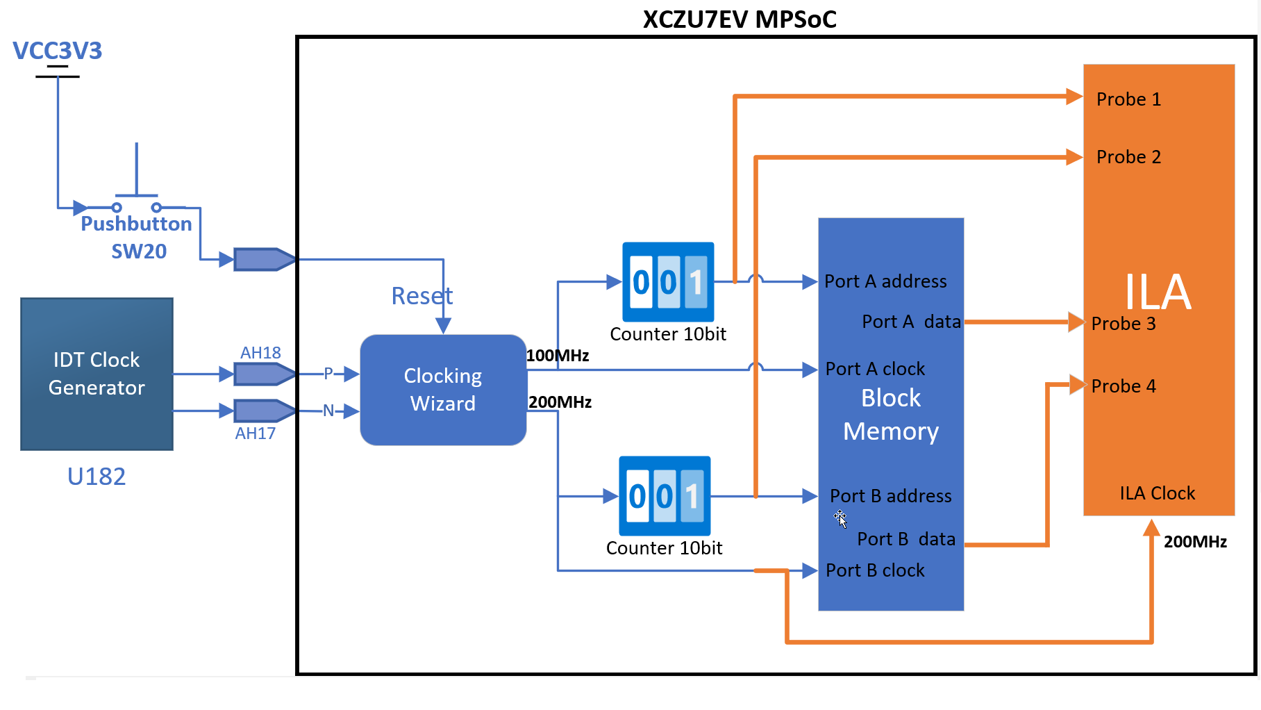
Block diagram of designThis figure shows the block diagram of design in Vivado:
Let’s have a look at the different section of design.
Clock Generation:
- IDT Clock Generator (U182):
- The IDT Clock Generator is responsible for providing the main clock signals that drive the system. It has differential clock outputs labeled P (AH18) and N (AH17). These signals are fed into the Clocking Wizard.
- Clocking Wizard:
- The ClockingWizard is a block that takes the clock input from the IDT Clock Generator and generates two output clock frequencies: 100 MHz and 200MHz. These are used by other components in the design.
- A pushbutton (SW20) is connected to a reset signal, allowing the system to be reset manually.
2. Address Generation:
- Two 10-bit counters are used to generate addresses for the Block Memory module.
- One counter is clocked by the 100 MHz clock (from the Clocking Wizard).
- The other counter is clocked by the 200 MHz clock.
- These counters generate sequential addresses for Port A and Port B of the Block Memory. The addresses are 10 bits wide, meaning they can address up to 1024 memory locations.
3. Block Memory:
- The Block Memory module has two independent ports (Port A and Port B), both of which can be accessed simultaneously.
- Port A:
- Receives the 10-bit address from the 100 MHz counter.
- Uses the 100 MHz clock to read/write data from/to this address.
- Port B:
- Receives the 10-bit address from the 200 MHz counter.
- Uses the 200 MHz clock for data operations.
- The Block Memory acts as a lookup table (LUT) where the sine wave data is stored. Based on the incoming addresses, the corresponding data is retrieved from memory and sent to other parts of the design.
- The Integrated Logic Analyzer (ILA) is used for monitoring and debugging signals inside the FPGA. In this diagram.
Start by creating a new project for the ZCU104 board, and then add a block design. Within the block design, use the "Add IP" feature to insert a Block Memory Generator.To configure the block memory, double-click on the Block Memory Generator block.
In the Basic tab, you’ll find two controller operation modes for the block memory. Since for this tutorial, we will be directly accessing and reading back buffered data from the block memory. Therefore, select the Native Interface, Stand-Alone Mode option.
For the Memory Type, this tutorial uses Block RAM as a lookup table to store pre-calculated sine wave values. These values are then read from the Block RAM to generate the sine wave. Additionally, we aim to explore how to operate two independent ports with different frequencies. To achieve this, we will use Dual-Port Read-Only Memory (ROM), which allows each port to operate independently, reading data at different clock rates.
Next, we open the Port A and Port B options tabs to configure the appropriate bit width and depth for storing the sine wave coefficients.
We choose 11 bits for each port, the Reason is that we are generating sine wave coefficients with 10-bit resolution for amplitude and an additional sign bit, (for positive/negative values). Therefore, the total bit width required to store each sine sample is 11 bits, (10 bits for magnitude + 1 bit for sign).
The depth of the memory defines how many different data values can be stored. Since we are generating 1024 sine wave coefficients, you need a depth of 1024 to store all these values
Additionally, we want both ports to remain continuously active, so we set the Enable Port Type to Always Enabled. This ensures that the ports are always ready for read and write operations without requiring external control signals to enable them.
we deselect the Primitive Output Register option. This reduces the Block RAM latency to 1 clock cycle, simplifying the design and making the result easier to understand by minimizing delays.
Open other options tab to load a memory initialization Coefficient file. This Coefficient file is used to pre-load BRAM in an FPGA design with specific initial data. When the design is synthesized and implemented, the Block RAM will contain the values provided in the file.
Now press the brows button and load the COE file. You can validate and then save it.
The block memory is now ready, and we will proceed to add additional IPs to the design.
- Add Programmable Differential Clock (300MHz):
- From the “Board” tab list, add a Programmable Differential Clock (300MHz). This will add a clock wizard with a differential input and connect it to the appropriate external pins.
After that you will find clocking wizard with connected input to external differential clock is added to your design:
Add Reset:
- From the “Board” tab list, add a reset and connect it to the reset pin of the clocking wizard.
- Note that when using the board examples, the board files’ pre-setups are automatically used. For example, based on the board pre-setups, the differential input is connected to I/O pins AH17 and AH18, which are connected to the 300MHz clock, and the reset input is connected to the M11 I/O pin, which is the CPU reset pushbutton.
- Note: here for the ease of the job, I used the designs from board window. however if you are working with a board without the presets or board files, you can first add a Clocking wizard to your design and then make its inputs as external. then after synthesis, during I/O planning, you can assign proper pins to the clocking wizard inputs based on the datasheet of of your board.
Configure the Clocking Wizard:
- Double-click on the clocking wizard to open it.
- The clocking wizard setup will instantiate an MMCM block to fulfill the frequency synthesis requirements.
Set Output Frequencies:
- Go to the output tab and add two frequencies with values of 100MHz and 200MHz.
- Allow the clocking wizard to add the buffers for routing the clocks into the clock network.
Binary Counters: add two binary counters to the design and set the output bit-width of each one to 10.
- Connections:
- Connect the clock pin of Port A to the 100 MHz clock generator and link the output of the first binary counter to the address port for Port A.
- Repeat this process for Port B, connecting it to the second binary counter and the 200 MHz clock generator.
This configuration ensures that Port A operates with a 100 MHz clock while Port B runs at 200 MHz. Consequently, the address for Port A is generated at 100 MHz, and the address for Port B is generated at 200 MHz.
Integrated Logic Analyzer (ILA) Connections:
Add an ILAto the design to monitor the signals at the output of the Block Memory Generator. Double click on the ILA IP and set the number of ports to 4, and increase sample data depth 4096. It allows us to capture 4 cycles of fastest sine wave.
- Probe 0: Monitors the address generated by c_counter_binary_0 (Port A address).
- Probe 1: Monitors the data output from Port A of the BRAM (douta).
- Probe 2: Monitors the address generated by c_counter_binary_1 (Port B address).
- Probe 3: Monitors the data output from Port B of the BRAM (doutb).
The ILA is clocked by the 200 MHz clock (clk_out2), which is the faster of the two clock frequencies used in the design.
The ILA needs to capture and observe signals in the system. In this design, since some signals are operating at 200 MHz(specifically the address and data outputs of Port B of the Block Memory Generator), the ILA needs to sample these signals at the same or higher clock rate to accurately capture all transitions.
connect the address and data out of port A to probe zero and one respectively. Repeat the same connection for address and data out of Port B.
Create top HDL wrapper and let the Vivado to manage and auto handle it. after that you can procced to generate the bitstream.
Obtained resultsDownload the bitstream into the device over the USB JTAG. After that, the ILA dashboard will open.
You can press “Run trigger immediate”, it will capture 4096 samples and display them.
Right-click on the two simulated signals to change their settings. Set the radix to signed decimal and the waveform style to analog.
After these adjustments, you will observe two sine waves fluctuating at different frequencies.
Let’s take a closer look at the binary output counters and how their output can be interpreted as analog signals. Make the captured output of binary counter as analog. This ties into the core concept of a Numerically Controlled Oscillator (NCO).
The counter in your design, acts as a phase accumulator. As it increments, it effectively creates a digital ramp signal. This ramp signal represents a linearly increasing phase value, which is crucial in generating periodic waveforms, like sine waves when passed through a lookup table.


Comments
Please log in or sign up to comment.